Datasheet
Table Of Contents
- FEATURES
- Applications
- DESCRIPTION
- Absolute Maximum Ratings
- Recommended Operating Conditions
- Electrical Characteristics
- Setup and Timing Diagrams
- Functional Description
- Application Information
- TYPICAL APPLICATION
- MULTIPLE HOP APPLICATION
- MATRIX SWITCH APPLICATION
- DUAL LINK APPLICATION
- DC AND AC COUPLED APPLICATIONS
- CABLE SELECTION AND INTER-PAIR SKEW
- 28 AWG STP (SHIELDED TWIST PAIRS) DVI / HDMI CABLES RECOMMENDED EQ SETTINGS
- 24 AWG UTP (LOW SKEW UNSHIELDED TWIST PAIRS) CABLES
- General Recommendations
- Typical Performance Characteristics as a Repeater
- Revision History

DS34RT5110
SNLS310G –MARCH 2009–REVISED APRIL 2013
www.ti.com
Electrical Characteristics (continued)
Over recommended operating supply and temperature ranges unless otherwise specified. All parameters are ensured by test,
statistical analysis, or design unless otherwise specified
(1)
.
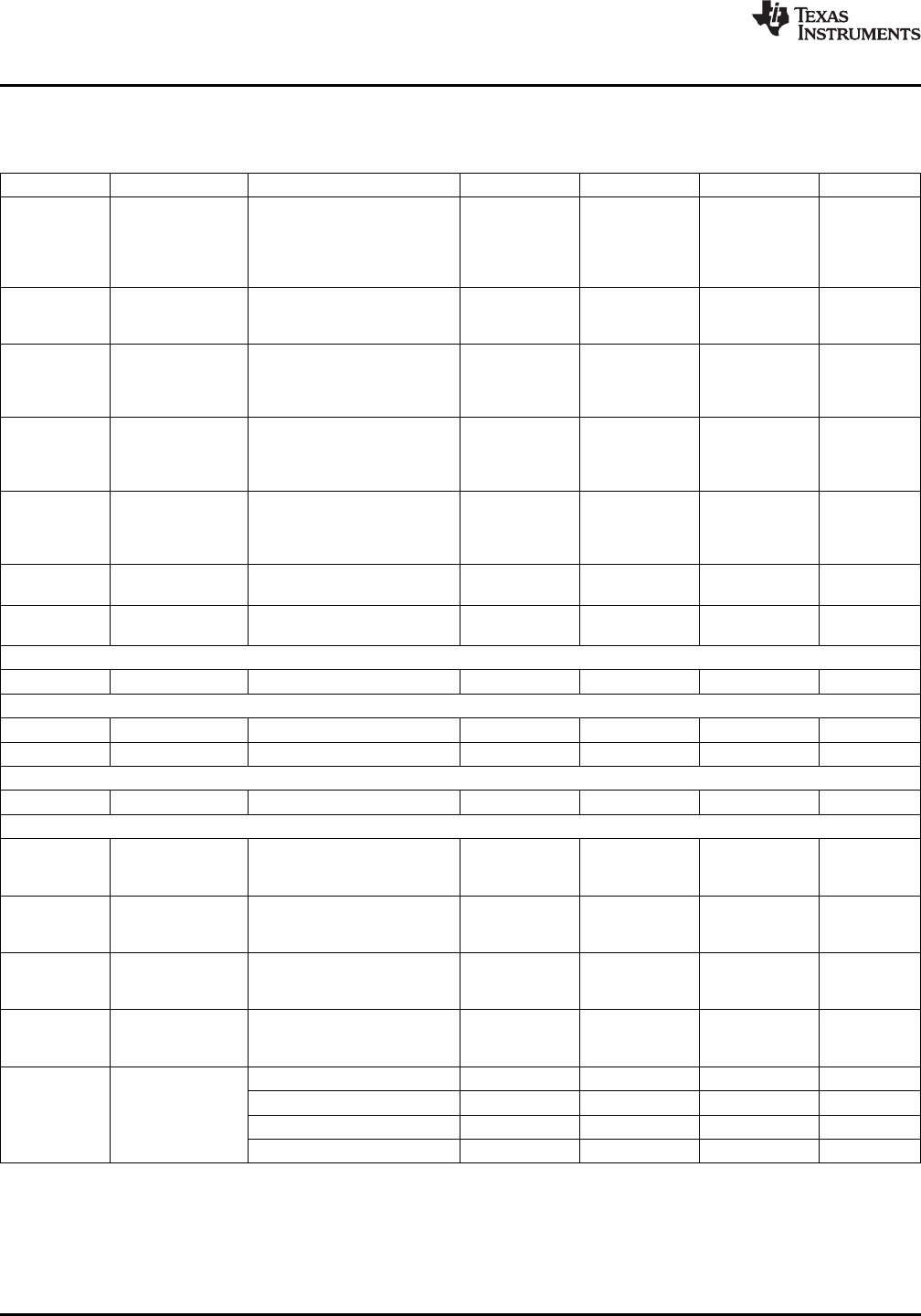
Symbol Parameter Condition Min Typ Max Units
External resistor = 24 kΩ at
VOD_CRL pin.Measured
Differential Output
VO differentially with OUT+ and 800 1200 mVp-p
voltage swing
OUT- terminated by RT=50Ω
to AV
CC
, Figure 2
Measured single-ended,
Output common-
VOCM >1.65 Gbps, Figure 2, AV
CC
- 0.35 AV
CC
- 0.20 V
mode Voltage
Figure 3
20% to 80% of differential
output voltage, measured
tR, tF Transition time 80 ps
within 1” from output pins,
Figure 3
Inter Pair Data
Difference in 50% crossing
Channel-to-
tCCSK between channels 2 3 ps
Channel Skew (all
3.4 Gbps, Clock Pattern
(2)
3 data channels)
Difference in 50% crossing
Inter Pair Data
between channels of any two
tPPSK Channels Part- 50 ps
devices
toPart Skew
3.4 Gbps, Clock Pattern
Data Channels 3.4 Gbps, Clock Pattern,
tDD 520 ps
Latency Figure 4
Clock Channel 3.4 Gbps, Clock Pattern,
tCD 600 ps
Latency Figure 4
LVCMOS Outputs
tSL SD to LOCK time Figure 4 10 ms
Bit Rate
fCLK Clock Frequency Clock Path
(3)
25 340 MHz
bR Bit Rate Data Paths
(3)
0.25 3.4 Gbps
Data Channel Random Jitter
RJ Random Jitter See
(3)(4)(5)(6)
3 psrms
Data Channel CDR Jitter Generation
Data Paths, measured at TPC
Total Output Jitter
TROJ1 PRBS7, EQ [2:0] = 000 0.03 0.05 UIp-p
0.25 Gbps
Figure 1
(3)(4)(5)
Data Paths, measured at TPC
Total Output Jitter
TROJ2 PRBS7, EQ [2:0] = 000 0.08 0.14 UIp-p
1.65 Gbps
Figure 1
(3)(4)(5)
Data Paths, measured at TPC
Total Output Jitter
TROJ3 PRBS7, EQ [2:0] = 000 0.09 0.16 UIp-p
2.25 Gbps
Figure 1
(3)(4)(5)
Data Paths, measured at TPC
Total Output Jitter
TROJ4 PRBS7, EQ [2:0] = 000 0.10 0.17 UIp-p
3.4 Gbps
Figure 1
(3)(4)(5)
0.25 Gbps data rate 0.25 MHz
1.65 Gbps data rate 1.65 MHz
CDR Loop
BWLOOP
Bandwidth
2.25 Gbps data rate 2.25 MHz
3.4 Gbps data rate 2.25 MHz
(3) Parameter is ensured by statistical analysis and/or design.
(4) Deterministic jitter is measured at the differential outputs (TPC of Figure 1), minus the deterministic jitter before the test channel (TPA of
Figure 1). Random jitter is removed through the use of averaging or similar means.
(5) Total Jitter is defined as peak-to-peak deterministic jitter from + 12 times random jitter (ps).
(6) Random jitter contributed by the equalizer is defined as sq rt (J
OUT
2
− J
IN
2
). J
OUT
is the random jitter at equalizer outputs in ps-rms, see
TPC of Figure 1; J
IN
is the random jitter at the input of the equalizer in ps-rms, see TPA of Figure 1.
6 Submit Documentation Feedback Copyright © 2009–2013, Texas Instruments Incorporated
Product Folder Links: DS34RT5110


