
Datasheet


Table Of Contents
- FEATURES
- Applications
- DESCRIPTION
- Absolute Maximum Ratings
- Recommended Operating Conditions
- Electrical Characteristics
- Setup and Timing Diagrams
- Functional Description
- Application Information
- TYPICAL APPLICATION
- MULTIPLE HOP APPLICATION
- MATRIX SWITCH APPLICATION
- DUAL LINK APPLICATION
- DC AND AC COUPLED APPLICATIONS
- CABLE SELECTION AND INTER-PAIR SKEW
- 28 AWG STP (SHIELDED TWIST PAIRS) DVI / HDMI CABLES RECOMMENDED EQ SETTINGS
- 24 AWG UTP (LOW SKEW UNSHIELDED TWIST PAIRS) CABLES
- General Recommendations
- Typical Performance Characteristics as a Repeater
- Revision History
10
11
12
13
14
15
16
17
18
19
20
21
22
23
24
36
35
34
33
32
31
30
29
28
27
26
25
48
47
46
45
44
43
42
41
40
39
38
37
1
2
3
4
5
6
7
8
9
DAP = GND
DS34RT5110
(Top View)
D_IN2+
D_IN2-
D_IN1+
D_IN1-
D_IN0+
D_IN0-
C_IN+
C_IN-
D_OUT2+
D_OUT2-
D_OUT1+
D_OUT1-
D_OUT0+
D_OUT0-
C_OUT+
C_OUT-
VDD
VDD
VDD
VDD
GND
GND
GND
GND
VDD
VDD
GND
GND
EQ1
EQ0
BYPASS
VDD
SD
EN
LFn
DE0
DE1
LFp
VOD_CRL
EQ2
Reserv
Reserv
LOCK
MODE
Reserv
Reserv
Reserv
Reserv
DS34RT5110
www.ti.com
SNLS310G –MARCH 2009–REVISED APRIL 2013
PIN DESCRIPTIONS (continued)
Pin Name Pin Number I/O, Type Description
LOCK 14 O, LVCMOS Lock Indicator Output pin.
H = PLL is locked.
L = PLL is not locked.
VOD_CRL 48 I, VOD control pin. Refer to Table 3. See Functional Description.
Analog External resistance = 24 kΩ to GND, Output DC Coupled Application.
External resistance = 12 kΩ to GND, Output AC Coupled Application.
LFp 40 I, Loop filter capacitor pins.
LFn 41 Analog See Functional Description.
Power
V
DD
3, 6, 7, Power V
DD
= 3.3 V ±5%. V
DD
pins should be tied to the V
DD
plane through a low inductance path. A
10, 13, 0.1 µF bypass capacitor should be connected between each V
DD
pin to the GND planes. See
15, 46 POWER SUPPLY BYPASSING for additional details.
GND 22, 24, GND Ground reference. GND should be tied to a solid ground plane through a low impedance
27, 30, path.
31, 34
Exposed DAP GND Ground reference. The exposed pad at the center of the package must be connected to the
DAP ground plane.
Other
Reserv 16, 17, Reserved. Do not connect. Leave open.
18, 19,
20, 23
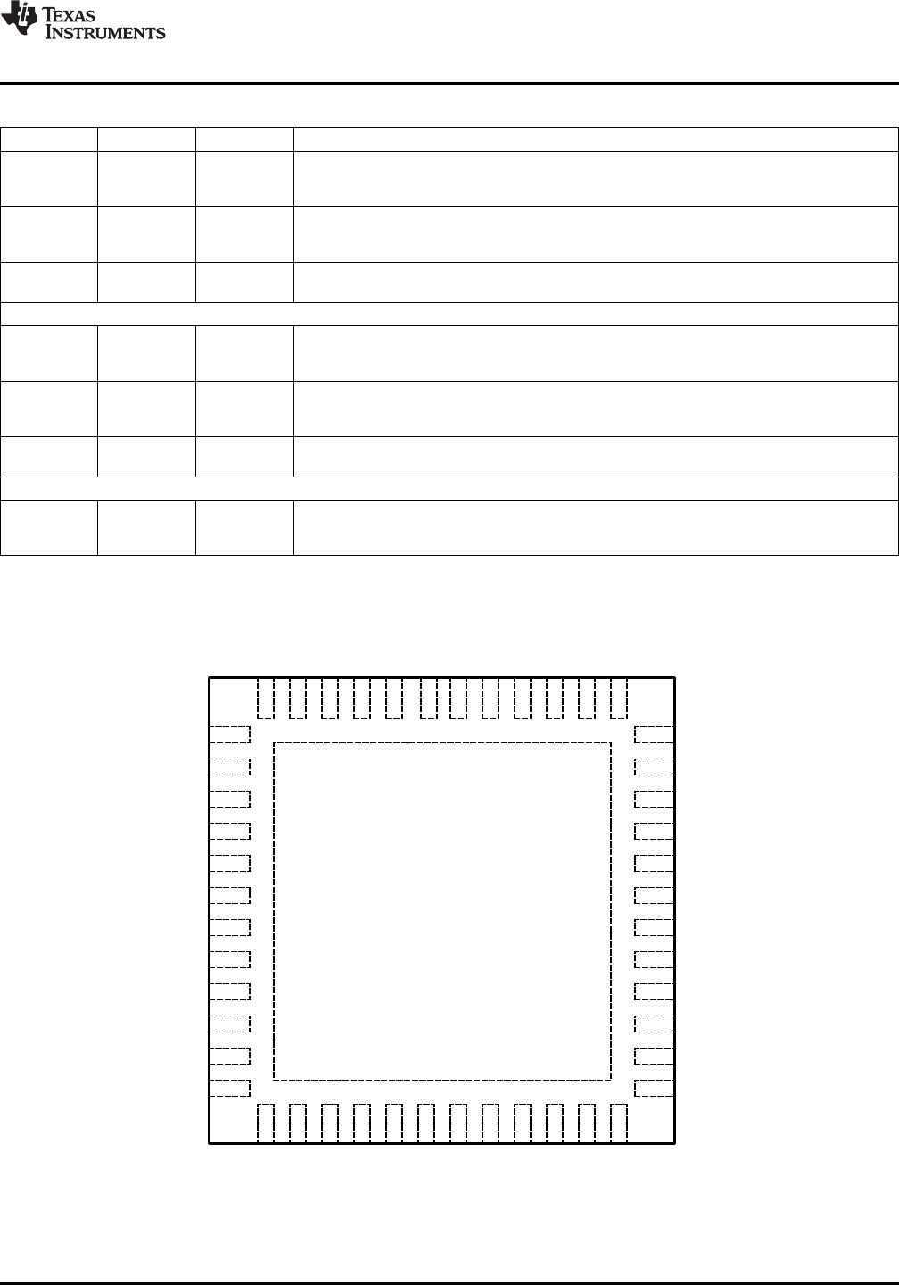
Connection Diagram
TOP VIEW — Not to Scale
48 Pin WQFN Package
See Package Number RHS0048A
Copyright © 2009–2013, Texas Instruments Incorporated Submit Documentation Feedback 3
Product Folder Links: DS34RT5110