
Datasheet


Table Of Contents
- FEATURES
- Applications
- DESCRIPTION
- Absolute Maximum Ratings
- Recommended Operating Conditions
- Electrical Characteristics
- Setup and Timing Diagrams
- Functional Description
- Application Information
- TYPICAL APPLICATION
- MULTIPLE HOP APPLICATION
- MATRIX SWITCH APPLICATION
- DUAL LINK APPLICATION
- DC AND AC COUPLED APPLICATIONS
- CABLE SELECTION AND INTER-PAIR SKEW
- 28 AWG STP (SHIELDED TWIST PAIRS) DVI / HDMI CABLES RECOMMENDED EQ SETTINGS
- 24 AWG UTP (LOW SKEW UNSHIELDED TWIST PAIRS) CABLES
- General Recommendations
- Typical Performance Characteristics as a Repeater
- Revision History
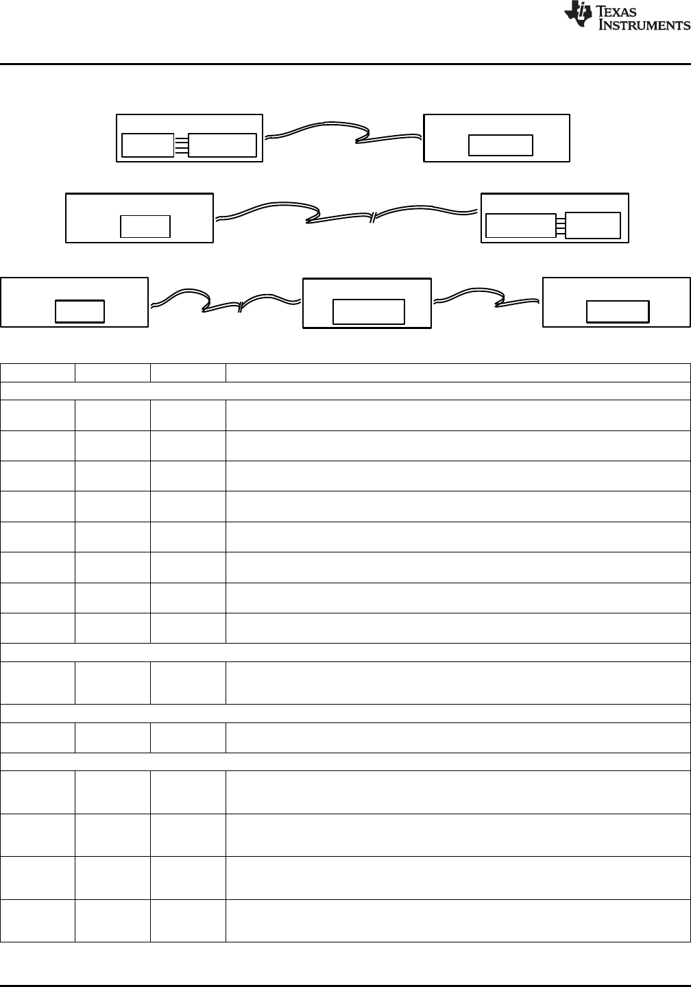
DES/Display
Processor
10.2 G DVI/HDMI Sink
5m 28 AWG DVI/HDMI Cable
DS34RT5110
DS34RT5110
DES/Display
Processor
10.2 G DVI/HDMI Sink
20m 28 AWG DVI/HDMI Cable
SER/A/V
Decoder
10.2 G DVI/HDMI Source
SER A/V
Decoder
10.2 G DVI/HDMI Source
20m 28 AWG DVI/HDMI Cable
DS34RT5110
DVI/HDMI Repeater
5m 28 AWG DVI/HDMI Cable
10.2 G DVI/HDMI Sink
DES/Display
Processor
10.2 G DVI/HDMI Source
SER/A/V
Decoder
DS34RT5110
SNLS310G –MARCH 2009–REVISED APRIL 2013
www.ti.com
Application Diagram
PIN DESCRIPTIONS
Pin Name Pin Number I/O, Type Description
High Speed Differential I/O
C_IN− 1 I, CML Inverting and non-inverting TMDS Clock inputs to the equalizer. An on-chip 50 Ω terminating
C_IN+ 2 resistor connects C_IN+ to V
DD
and C_IN- to V
DD
.
D_IN0− 4 I, CML Inverting and non-inverting TMDS Data inputs to the equalizer. An on-chip 50 Ω terminating
D_IN0+ 5 resistor connects D_IN0+ to V
DD
and D_IN0- to V
DD
.
D_IN1− 8 I, CML Inverting and non-inverting TMDS Data inputs to the equalizer. An on-chip 50 Ω terminating
D_IN1+ 9 resistor connects D_IN1+ to V
DD
and D_IN1- to V
DD
.
D_IN2− 11 I, CML Inverting and non-inverting TMDS Data inputs to the equalizer. An on-chip 50 Ω terminating
D_IN2+ 12 resistor connects D_IN2+ to V
DD
and D_IN2- to V
DD
.
C_OUT- 36 O, CML Inverting and non-inverting TMDS outputs from the equalizer. Open collector.
C_OUT+ 35
D_OUT0− 33 O, CML Inverting and non-inverting TMDS outputs from the equalizer. Open collector.
D_OUT0+ 32
D_OUT1– 29 O, CML Inverting and non-inverting TMDS outputs from the equalizer. Open collector.
D_OUT1+ 28
D_OUT2− 26 O, CML Inverting and non-inverting TMDS outputs from the equalizer. Open collector.
D_OUT2+ 25
Equalization Control
EQ2 37 I, LVCMOS EQ2, EQ1 and EQ0 select the equalizer boost level for EQ channels. Internally pulled LOW
EQ1 38 as default. Refer to Table 1.
EQ0 39
De-Emphasis Control
DE1 42 I, DE1, DE0 select the DE-emphasis level for output drivers. Internally pulled low as default.
DE0 43 LVCMOS Refer to Table 2.
Device Control
BYPASS 47 I, Reclocker enable control. Internally pulled low as default.
LVCMOS H = Reclock and De-Emphasis function is bypassed.
L = Normal operation.
EN 44 I, LVCMOS Enable Output Drivers. Internally pulled HIGH as default.
H = normal operation (enabled).
L = standby mode.
MODE 21 I, LVCMOS Clock channel mode control. Internally pulled LOW as default.
H = Clock channel is bypassed.
L = Normal operation.
SD 45 O, LVCMOS Signal Detect Output pin.
H = signal detected on all channels.
L = no signal detected on one or more channels.
2 Submit Documentation Feedback Copyright © 2009–2013, Texas Instruments Incorporated
Product Folder Links: DS34RT5110