
Datasheet


Table Of Contents
- FEATURES
- Applications
- DESCRIPTION
- Absolute Maximum Ratings
- Recommended Operating Conditions
- Electrical Characteristics
- Setup and Timing Diagrams
- Functional Description
- Application Information
- TYPICAL APPLICATION
- MULTIPLE HOP APPLICATION
- MATRIX SWITCH APPLICATION
- DUAL LINK APPLICATION
- DC AND AC COUPLED APPLICATIONS
- CABLE SELECTION AND INTER-PAIR SKEW
- 28 AWG STP (SHIELDED TWIST PAIRS) DVI / HDMI CABLES RECOMMENDED EQ SETTINGS
- 24 AWG UTP (LOW SKEW UNSHIELDED TWIST PAIRS) CABLES
- General Recommendations
- Typical Performance Characteristics as a Repeater
- Revision History
505
VDD
505
OUT+
OUT-
+ Clamp
Circuitry
DS34RT5110
SNLS310G –MARCH 2009–REVISED APRIL 2013
www.ti.com
PCB LAYOUT CONSIDERATIONS FOR DIFFERENTIAL PAIRS
The TMDS differential inputs and outputs must have a controlled differential impedance of 100 Ω. It is preferable
to route TMDS lines exclusively on one layer of the board, particularly for the input traces. The use of vias should
be avoided if possible. If vias must be used, they should be used sparingly and must be placed symmetrically for
each side of a given differential pair. Route the TMDS signals away from other signals and noise sources on the
printed circuit board. All traces of TMDS differential inputs and outputs must be equal in length to minimize intra-
pair skew.
WQFN FOOTPRINT RECOMMENDATIONS
See TI application note: AN-1187 “Leadless Leadframe Package (LLP) Application Report” (literature number
SNOA401) for additional information on WQFN packages footprint and soldering information.
POWER SUPPLY BYPASSING
Two approaches are recommended to ensure the DS34RT5110 is provided with an adequate power supply.
First, the supply (VDD) and ground (GND) pins should be connected to power planes routed on adjacent layers
of the printed circuit board. The layer thickness of the dielectric should be minimized so the VDD and GND
planes create a low inductance supply with distributed capacitance. Second, careful attention to supply
bypassing through the proper use of bypass capacitors is required. A 0.1 μF bypass capacitor should be
connected to each VDD pin such that the capacitor is placed as close as possible to the DS34RT5110. Smaller
body size capacitors can help facilitate proper component placement. Additionally, two capacitors with
capacitance in the range of 2.2 μF to 10 μF should be incorporated in the power supply bypassing design as
well. These capacitors can be either tantalum or an ultra-low ESR ceramic and should be placed as close as
possible to the DS34RT5110.
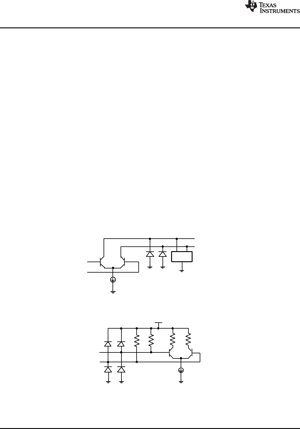
EQUIVALENT I/O STRUCTURES
Figure 14 shows the DS34RT5110 CML output structure and ESD protection circuitry.
Figure 15 shows the DS34RT5110 CML input structure and ESD protection circuitry.
Figure 14. Equivalent Output Structure
Figure 15. Equivalent Input Structure
16 Submit Documentation Feedback Copyright © 2009–2013, Texas Instruments Incorporated
Product Folder Links: DS34RT5110