
Datasheet


Table Of Contents
- FEATURES
- Applications
- DESCRIPTION
- Absolute Maximum Ratings
- Recommended Operating Conditions
- Electrical Characteristics
- Setup and Timing Diagrams
- Functional Description
- Application Information
- TYPICAL APPLICATION
- MULTIPLE HOP APPLICATION
- MATRIX SWITCH APPLICATION
- DUAL LINK APPLICATION
- DC AND AC COUPLED APPLICATIONS
- CABLE SELECTION AND INTER-PAIR SKEW
- 28 AWG STP (SHIELDED TWIST PAIRS) DVI / HDMI CABLES RECOMMENDED EQ SETTINGS
- 24 AWG UTP (LOW SKEW UNSHIELDED TWIST PAIRS) CABLES
- General Recommendations
- Typical Performance Characteristics as a Repeater
- Revision History
505
VDD
505
Zo
DS34RT5110
Driver
DS34RT5110
Receiver
24 k5
VOD_CRL
24 k5
VOD_CRL
DS34RT5110
DS34RT5110
D0
D1
D2
CLK
D3
D4
D5
D0
D1
D2
CLK
D3
D4
D5
CLK
MODE = 0 (Default)
MODE = 1
DS34RT5110
SNLS310G –MARCH 2009–REVISED APRIL 2013
www.ti.com
Figure 11. DVI/HDMI Dual Link Application
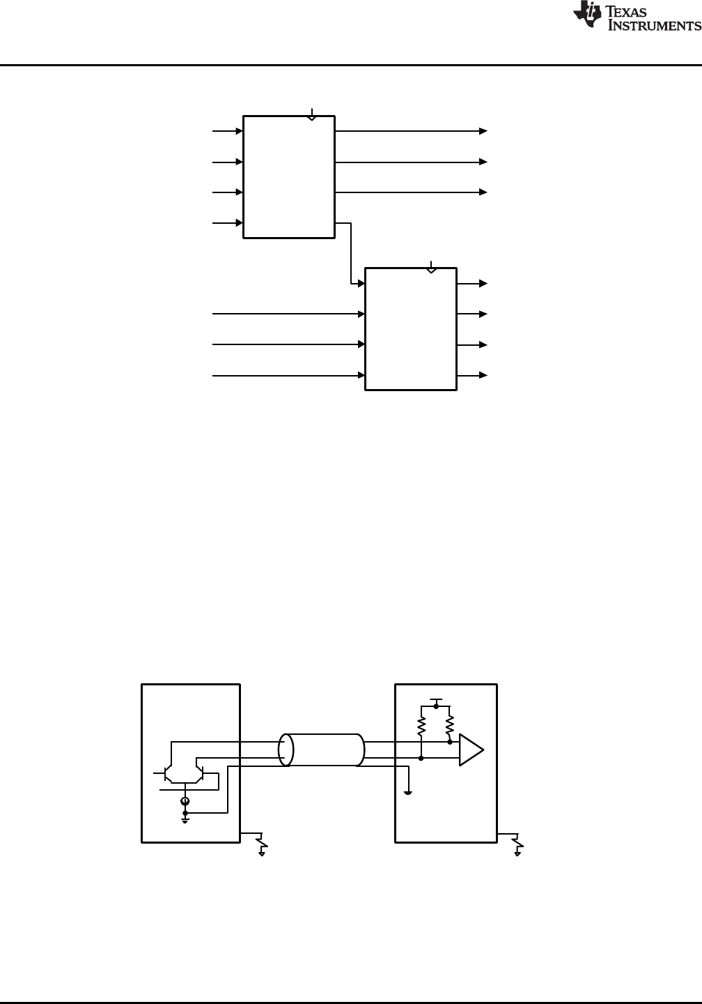
DC AND AC COUPLED APPLICATIONS
The DS34RT5110 is designed to support TMDS differential pairs with DC coupled transmission lines. It contains
integrated termination resistors (50Ω), pulled up to VDD at the input stage, and open collector outputs for DVI /
HDMI signaling. Figure 12 shows the DC coupled connection between the HDMI Source (ie. DS34RT5110) and
HDMI Sink (ie. DS34RT5110) devices. In the DC coupled application, the external resistance of 24 kΩ at
VOD_CRL pin is used at the Source to ensure the VO level of 1000 mVp-p. The AC coupled method connecting
between the Source and the Sink devices may be preferred to eliminate the impact of the ground potential
difference, or to use one CAT5/6 cable between two chassis. To optimize the DS34RT5110 performance, the
external resistance of 12 kΩ at the VOD_CRL pin should be used on the Source DS34RT5110, and a pair of 50
Ω pull-up resistors should be placed close to the outputs of the Source DS34RT5110, in order to DC bias the
output driver. Meanwhile, 622Ω pull-down resistors should be placed at the inputs of the Sink DS34RT5110
device, in order to set the input common mode to a 3.05 V. Note AC coupled configuration is not compliant to the
HDMI specification of Source requirement (See Figure 13).
Figure 12. DC Coupled Application
14 Submit Documentation Feedback Copyright © 2009–2013, Texas Instruments Incorporated
Product Folder Links: DS34RT5110