
Datasheet


Table Of Contents
- FEATURES
- Applications
- DESCRIPTION
- Absolute Maximum Ratings
- Recommended Operating Conditions
- Electrical Characteristics
- Setup and Timing Diagrams
- Functional Description
- Application Information
- TYPICAL APPLICATION
- MULTIPLE HOP APPLICATION
- MATRIX SWITCH APPLICATION
- DUAL LINK APPLICATION
- DC AND AC COUPLED APPLICATIONS
- CABLE SELECTION AND INTER-PAIR SKEW
- 28 AWG STP (SHIELDED TWIST PAIRS) DVI / HDMI CABLES RECOMMENDED EQ SETTINGS
- 24 AWG UTP (LOW SKEW UNSHIELDED TWIST PAIRS) CABLES
- General Recommendations
- Typical Performance Characteristics as a Repeater
- Revision History
VO
VODE3
VODE2
VODE1
1-bit 1 to N bits 1-bit 1 to N bits
0 dB
-3 dB
-6 dB
-9 dB
0V
DS34RT5110
www.ti.com
SNLS310G –MARCH 2009–REVISED APRIL 2013
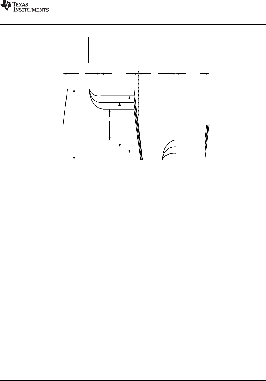
Table 3. VO Control
External Resistor Value
Applications VO Level (mVp-p)
(VOD_CRL pin)
24 kΩ DC Coupled 1000
12 kΩ AC Coupled 1000
Figure 7. Output De-Emphasis Differential Waveform (showing all de-emphasis steps)
RETIMING AND DE-EMPHASIS BYPASS
The retiming and De-emphasis BYPASS pin provides the flexibility to configure the device to an equalizer only
mode. The device is in normal operation, when holding a LOW state on the BYPASS pin. The retiming and De-
emphasis features are disabled, when a HIGH state is applied.
CLOCK CHANNEL MODE CONTROL
During the normal operation mode, the clock channel signal is regenerated by the PLL and the CDR. Holding a
LOW state (default) on the MODE pin places the DS34RT5110 in this normal operation mode. A HIGH state on
the MODE pin bypasses the clock channel. This clock channel mode feature enables the multi-hop applications.
(Refer to Multiple Hop Application for detailed information)
DEVICE STATE AND ENABLE CONTROL
The DS34RT5110 has an Enable feature which provides the ability to control device power consumption. This
feature can be controlled via the Enable Pin (EN Pin). If Enable is activated, the data channels and clock channel
are placed in the ACTIVE state and all device blocks function as described. The DS34RT5110 can also be
placed in STANDBY mode to save power. In this mode, the output drivers of the device are disabled. The CML
outputs are in the HIGH (AVCC) state. All LVCMOS outputs are in the HiZ state.
LOCK DETECT
When the PLL of the DS34RT5110 is locked, and the generated reference phases are successfully interpolated
by the CDR, this status is indicated by a logic HIGH on the LOCK pin. The LOCK pin may be connected to the
Enable (EN) pin input to disable the data channels and clock channel when no data signal is being received.
SIGNAL DETECT
The DS34RT5110 features a signal detect circuit on all channels. The status of the input signals can be
determined by the state of the SD pin. A logic HIGH indicates the presence of signals that have exceeded a
specified maximum threshold value (called SD_ON) on all channels. A logic LOW means that the signals have
fallen below a minimum threshold value (called SD_OFF) on one or more channels.
Copyright © 2009–2013, Texas Instruments Incorporated Submit Documentation Feedback 11
Product Folder Links: DS34RT5110