
Datasheet


DRV8836
SLVSB17B –MARCH 2012–REVISED JANUARY 2014
www.ti.com
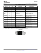
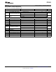
ABSOLUTE MAXIMUM RATINGS
(1)(2)
VALUE UNIT
VCC Power supply voltage range -0.3 to 7 V
Digital input pin voltage range –0.5 to VCC + 0.5 V
Peak motor drive output current Internally limited A
Continuous motor drive output current per H-bridge
(3)
1.5 A
T
J
Operating junction temperature range –40 to 150 °C
T
stg
Storage temperature range –60 to 150 °C
(1) Stresses beyond those listed under absolute maximum ratings may cause permanent damage to the device. These are stress ratings
only, and functional operation of the device at these or any other conditions beyond those indicated under recommended operating
conditions is not implied. Exposure to absolute–maximum–rated conditions for extended periods may affect device reliability.
(2) All voltage values are with respect to network ground terminal.
(3) Power dissipation and thermal limits must be observed.
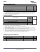
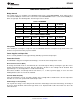
THERMAL INFORMATION
DRV8836
THERMAL METRIC DSS UNITS
12 PINS
θ
JA
Junction-to-ambient thermal resistance
(1)
50.4
θ
JCtop
Junction-to-case (top) thermal resistance
(2)
58
θ
JB
Junction-to-board thermal resistance
(3)
19.9
°C/W
ψ
JT
Junction-to-top characterization parameter
(4)
0.9
ψ
JB
Junction-to-board characterization parameter
(5)
20
θ
JCbot
Junction-to-case (bottom) thermal resistance
(6)
6.9
(1) The junction-to-ambient thermal resistance under natural convection is obtained in a simulation on a JEDEC-standard, high-K board, as
specified in JESD51-7, in an environment described in JESD51-2a.
(2) The junction-to-case (top) thermal resistance is obtained by simulating a cold plate test on the package top. No specific JEDEC-
standard test exists, but a close description can be found in the ANSI SEMI standard G30-88.
(3) The junction-to-board thermal resistance is obtained by simulating in an environment with a ring cold plate fixture to control the PCB
temperature, as described in JESD51-8.
(4) The junction-to-top characterization parameter, ψ
JT
, estimates the junction temperature of a device in a real system and is extracted
from the simulation data for obtaining θ
JA
, using a procedure described in JESD51-2a (sections 6 and 7).
(5) The junction-to-board characterization parameter, ψ
JB
, estimates the junction temperature of a device in a real system and is extracted
from the simulation data for obtaining θ
JA
, using a procedure described in JESD51-2a (sections 6 and 7).
(6) The junction-to-case (bottom) thermal resistance is obtained by simulating a cold plate test on the exposed (power) pad. No specific
JEDEC standard test exists, but a close description can be found in the ANSI SEMI standard G30-88.
Spacer
xxx
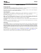
RECOMMENDED OPERATING CONDITIONS
T
A
= 25°C (unless otherwise noted)
MIN NOM MAX UNIT
V
CC
Device power supply voltage range 2 7 V
I
OUT
H-bridge output current
(1)
0 1.5 A
f
PWM
Externally applied PWM frequency 0 250 kHz
V
IN
Logic level input voltage 0 V
CC
V
(1) Power dissipation and thermal limits must be observed.
4 Submit Documentation Feedback Copyright © 2012–2014, Texas Instruments Incorporated
Product Folder Links: DRV8836