
Datasheet
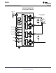

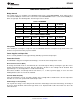


Over-
Temp
AOUT1
AOUT2
GND
MODE
AIN1/APHASE
AIN2/AENBL
VCC
VCC
VCC
2.0 to 7V
Gate
Drive
Logic
Osc
OCP
VCC
Gate
Drive
OCP
BOUT1
BOUT2
VCC
Gate
Drive
OCP
VCC
Gate
Drive
OCP
BIN1/BPHASE
BIN2/BENBL
Step
Motor
Drives 2x DC motor
or 1x Stepper
DCM
DCM
nSLEEP
Charge
Pump
DRV8836
SLVSB17B –MARCH 2012–REVISED JANUARY 2014
www.ti.com
DEVICE INFORMATION
Functional Block Diagram
2 Submit Documentation Feedback Copyright © 2012–2014, Texas Instruments Incorporated
Product Folder Links: DRV8836