
Datasheet


www.ti.com
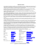
Connectors
4 Connectors
4.1 Motor Outputs
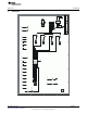
The connector J2 should be connected to the motor terminals. Each pin in this terminal is labeled on the
EVM itself as AOUT1, AOUT2, BOUT1 and BOUT2. The polarity of these connections will affect the
direction of the motor in the case of a brushed DC motor. In case of a stepper motor, one winding should
be connected to AOUT1 and AOUT2, while the other should be connected to the outputs BOUT1 and
BOUT2. Refer the datasheet for further information.
4.2 Power and Control Signals
The power and control signals for the DRV8833 are applied through the connector J1. Each pin in the
connector is labeled on the EVM. Check the schematic for further clarification. The control signals for
AIN1, AIN2, BIN1 and BIN2 can also be generated on board. Refer the Jumpers section in this user guide.
The connector J1 also outputs the nFAULT signal from the IC and the VDD (5 V) generated from the
on-board voltage regulator. These signals are labeled on the EVM silkscreen.
Apply a power of 2.7 V – 10.8 V between VM and GND on J1. Be sure to observe the correct polarity.
5 Jumpers
5.1 Voltage Regulator (JP6)
For the purpose of easy evaluation, a voltage regulator is provided on the DRV8833EVM. This regulator
regulates the VM voltage down to 5 V if VM is greater than 5 V and maintains VM if VM is less than 5 V. If
jumper JP6 is left shunted, the VDD signal on the board is provided by this regulator. It is 5 V and can
drive up to 150 mA. This signal is used to light up the nFAULT LED, drive the nSLEEP signal and
generates the HI signal for the switches AIN1, AIN2, BIN1 and BIN2. If the sleep current of the DRV8833
is being evaluated, leave this shunt off the board. This would make sure that the current measurement
through VM doesn’t include the current to the voltage regulator.
5.2 nSLEEP (JP5)
If this jumper is shunted, the 5 V generated from the on-board voltage regulator is connected to the
nSLEEP pin. This ensures the part doesn’t enter the SLEEP mode. If the SLEEP mode is not being
evaluated, then the Jumper can be left shunted. If the SLEEP mode is being controlled externally through
any controller, then disconnect this jumper and connect the nSLEEP signal from the external controller
directly to the test point – nSLEEP.
5.3 xINx Signals (JP1, JP2, JP3 and JP4)
Jumpers JP1, JP2, JP3 and JP4 are used to select the source of the control signals AIN2, AIN1, BIN1 and
BIN2 respectively. By placing a shunt between positions 1-2, the source of these control signals are
routed to the connector J1. This connection allows the user to control these signals through an external
controller.
If the shunt is placed between positions 2-3, then the source of these control signals are routed to the
switches AIN1, AIN2, BIN1 and BIN2. Refer to the section on the Switches for more information.
6 Switches (AIN1, AIN2, BIN1 and BIN2)
When the jumpers JP1, JP2, JP3 and JP4 are set such that the control signals AIN1, AIN2, BIN1 and
BIN2 are routed to the switches, these switches can be used to control the state of these input signals.
The positions are labeled appropriately as HI and LO. LO is GND and HI is VDD (5 V). The state of the
motor outputs for various input combinations can be inferred from the datasheet.
7
SLVU498– July 2011 Contents
Submit Documentation Feedback
Copyright © 2011, Texas Instruments Incorporated