
Datasheet


Contents
1 Introduction ........................................................................................................................ 4
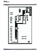
2 Schematic .......................................................................................................................... 5
3 PCB ................................................................................................................................... 6
4 Connectors ......................................................................................................................... 7
4.1 Motor Outputs ............................................................................................................ 7
4.2 Power and Control Signals ............................................................................................. 7
5 Jumpers ............................................................................................................................. 7
5.1 Voltage Regulator (JP6) ................................................................................................ 7
5.2 nSLEEP (JP5) ........................................................................................................... 7
5.3 xINx Signals (JP1, JP2, JP3 and JP4) ............................................................................... 7
6 Switches (AIN1, AIN2, BIN1 and BIN2) ................................................................................... 7
7 LED (D1) ............................................................................................................................ 8
8 Test Points ......................................................................................................................... 8
9 Current Sense Resistors (R5, R6) .......................................................................................... 8
3
SLVU498– July 2011 Table of Contents
Submit Documentation Feedback
Copyright © 2011, Texas Instruments Incorporated