
Datasheet
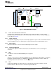

3.3-V Regulator
CN2 : VCC Output Connector
CN4 : 3.3-V Analog and Digital I/Os
CN3 : 5-V Analog and Digital I/Os
CN5 : VCC Output Connector
Level Shifters : 3.3 V 5.0 Vó
www.ti.com
Appendix B I/F Board
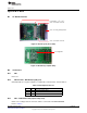
B.1 I/F Board Overview
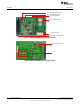
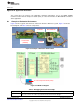
Figure 9. Board Layout (Front Side)
Figure 10. Board Layout (Back Side)
B.2 Connectors
B.2.1 CN1
Not used
B.2.2 CN2 and CN5 – B3B-XH-A(LF)(SN) (JST)
CN2 and CN5 are 5-V power supplies to components on the board or external devices.
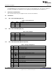
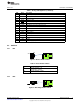
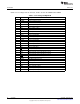
Table 7. VCC Output Connector
Pin# Name Description
1 VCC VCC power supply output
2 NC No connection
3 GND Ground
B.2.3 CN3 – FCN-365P032-AU (Fujitsu Component)
CN3 is a 5-V voltage level I/F connector, and It is connected on the DRV3204EVM.
Refer to Table 3.
9
SLVU844–February 2013 I/F Board
Submit Documentation Feedback
Copyright © 2013, Texas Instruments Incorporated