
Datasheet

Connectors and Switches
www.ti.com
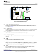
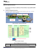
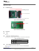
1.2.5 Test Pins
The DRV3204-Q1 pins are brought out to the test pin or test through-hole. For each test pin, a label on
the silkscreen identifies the signal. Access the signals by using 14 through-holes, marked as J1.
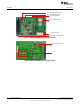
2 Connectors and Switches
This section describes the pin assignment of the connectors and switches.
2.1 Connectors
2.1.1 CN1 – B3P-VH-FB-B(LF)(SN) (JST)
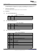
Table 1. Power Connectors
Pin# Name Description
1 VB External power supply (typ 12-V, max 10 A)
2 NC No connection
3 GND Base ground (B-GND)
2.1.2 CN2 – B5P-VH-FB-B(LF)(SN) (JST)
Table 2. Motor Outputs
Pin# Name Description
1 Motor1 Motor terminal 1
2 NC No Connection
3 Motor2 Motor terminal 2
4 NC No Connection
5 Motor3 Motor terminal 3
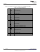
2.1.3 CN3 – FCN-365J032-AU (Fujitsu Component)
Table 3. Analog and Digital I/O
Pin# Name Description
A1 PMV1 Phase comparator output 1
B1 PMV2 Phase comparator output 2
A2 PMV3 Phase comparator output 3
B2 PSS1 Sample and hold control signal input 1 (not used)
A3 PSS2 Sample and hold control signal input 2 (not used)
B3 PSS3 Sample and hold control signal input 3 (not used)
A4 CS SPI chip select signal input
B4 DOUT SPI data signal output
A5 SCK SPI clock signal input
B5 DIN SPI data signal input
A6 CTLEN Pre-driver parallel enable input (not used)
B6 CTLWL Pre-driver parallel input
A7 CTLWH Pre-driver parallel input
B7 CTLVL Pre-driver parallel input
A8 CTLVH Pre-driver parallel input
B8 CTLUL Pre-driver parallel input
4
DRV3204-Q1 EVM SLVU844–February 2013
Submit Documentation Feedback
Copyright © 2013, Texas Instruments Incorporated