
Datasheet


Table Of Contents
- FEATURES
- APPLICATIONS
- DESCRIPTION
- PINOUT INFORMATION
- ABSOLUTE MAXIMUM RATINGS
- THERMAL INFORMATION
- RECOMMENDED OPERATING CONDITIONS
- ELECTRICAL CHARACTERISTICS
- TIMING REQUIREMENTS
- TYPICAL CHARACTERISTICS
- SYSTEM DIAGRAMS
- APPLICATION INFORMATION
- ECCENTRIC ROTATING MASS MOTORS (ERM)
- LINEAR RESONANCE ACTUATORS (LRA)
- AUTO-RESONANCE ENGINE FOR LRA
- OPEN LOOP OPERATION FOR LRA
- SMART LOOP ARCHITECTURE
- AUTO CALIBRATION
- WAVEFORM LIBRARIES
- WAVEFORM SEQUENCER
- LIBRARY PARAMETERIZATION
- REAL-TIME PLAYBACK (RTP) MODE
- MULTI-MODE INPUT PIN (IN/TRIG)
- DEVICE ENABLE
- CONSTANT VIBRATION STRENGTH
- EDGE RATE CONTROL
- CAPACITOR SELECTION
- MODES OF OPERATION
- BLOCK DIAGRAM
- GENERAL I2C OPERATION
- SINGLE-BYTE AND MULTIPLE-BYTE TRANSFERS
- SINGLE-BYTE WRITE
- MULTIPLE-BYTE WRITE AND INCREMENTAL MULTIPLE-BYTE WRITE
- SINGLE-BYTE READ
- MULTIPLE-BYTE READ
- REGISTER MAP
- DEVICE PROGRAMMING
- WAVEFORM LIBRARY EFFECTS LIST
- PCB LAYOUT RECOMMENDATIONS
- Revision History
Copper
Trace Width
Solder Mask
Thickness
Solder
Pad Width
Solder Mask
Opening
Copper Trace
Thickness
DRV2605
www.ti.com
SLOS825B –DECEMBER 2012–REVISED JANUARY 2014
PCB LAYOUT RECOMMENDATIONS
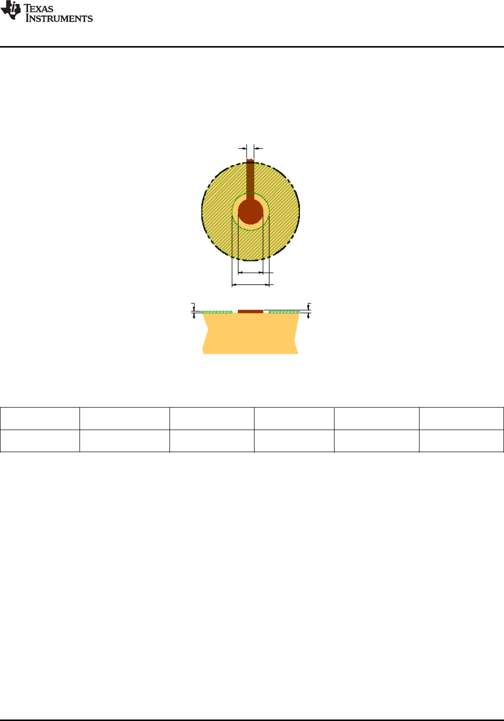
In making the pad size for the WCSP balls, it is recommended that the layout use nonsolder mask defined
(NSMD) land. With this method, the solder mask opening is made larger than the desired land area, and the
opening size is defined by the copper pad width. Figure 24 and Table 2 show the appropriate diameters for a
WCSP layout. The TPA2010D1 evaluation module (EVM) layout is shown in the next section as a layout
example.
Figure 24. Land Pattern Dimensions
Table 2. Land Pattern Dimensions
SOLDER PAD SOLDER MASK COPPER STENCIL STENCIL
COPPER PAD
DEFINITIONS OPENING THICKNESS OPENING THICKNESS
Nonsolder mask 275 μm 375 μm 1 oz max (32 μm) 275 μm x 275 μm Sq. 125 μm thick
defined (NSMD) (+0.0, –25 μm) (+0.0, –25 μm) (rounded corners)
NOTES:
1. Circuit traces from NSMD defined PWB lands should be 75 μm to 100 μm wide in the exposed area inside
the solder mask opening. Wider trace widths reduce device stand off and impact reliability.
2. Recommend solder paste is Type 3 or Type 4.
3. Best reliability results are achieved when the PWB laminate glass transition temperature is above the
operating the range of the intended application.
4. For a PWB using a Ni/Au surface finish, the gold thickness should be less 0.5 μm to avoid a reduction in
thermal fatigue performance.
5. Solder mask thickness should be less than 20 μm on top of the copper circuit pattern.
6. Best solder stencil performance is achieved using laser cut stencils with electro polishing. Use of chemically
etched stencils results in inferior solder paste volume control.
7. Trace routing away from WCSP device should be balanced in X and Y directions to avoid unintentional
component movement due to solder wetting forces.
Trace Width
Recommended trace width at the solder balls is 75 μm to 100 μm to prevent solder wicking onto wider PCB
traces. Maintain this trace width until the ball pattern is escaped, then the trace width may be increased for
improved current flow. The width/length of the 75 μm to 100 μm traces should be as symmetrical as possible
around the device to give even solder reflow on each of the balls.
Copyright © 2012–2014, Texas Instruments Incorporated Submit Documentation Feedback 43
Product Folder Links: DRV2605