
Datasheet


Table Of Contents
- FEATURES
- APPLICATIONS
- DESCRIPTION
- PINOUT INFORMATION
- ABSOLUTE MAXIMUM RATINGS
- THERMAL INFORMATION
- RECOMMENDED OPERATING CONDITIONS
- ELECTRICAL CHARACTERISTICS
- TIMING REQUIREMENTS
- TYPICAL CHARACTERISTICS
- SYSTEM DIAGRAMS
- APPLICATION INFORMATION
- ECCENTRIC ROTATING MASS MOTORS (ERM)
- LINEAR RESONANCE ACTUATORS (LRA)
- AUTO-RESONANCE ENGINE FOR LRA
- OPEN LOOP OPERATION FOR LRA
- SMART LOOP ARCHITECTURE
- AUTO CALIBRATION
- WAVEFORM LIBRARIES
- WAVEFORM SEQUENCER
- LIBRARY PARAMETERIZATION
- REAL-TIME PLAYBACK (RTP) MODE
- MULTI-MODE INPUT PIN (IN/TRIG)
- DEVICE ENABLE
- CONSTANT VIBRATION STRENGTH
- EDGE RATE CONTROL
- CAPACITOR SELECTION
- MODES OF OPERATION
- BLOCK DIAGRAM
- GENERAL I2C OPERATION
- SINGLE-BYTE AND MULTIPLE-BYTE TRANSFERS
- SINGLE-BYTE WRITE
- MULTIPLE-BYTE WRITE AND INCREMENTAL MULTIPLE-BYTE WRITE
- SINGLE-BYTE READ
- MULTIPLE-BYTE READ
- REGISTER MAP
- DEVICE PROGRAMMING
- WAVEFORM LIBRARY EFFECTS LIST
- PCB LAYOUT RECOMMENDATIONS
- Revision History
DRV2605
SLOS825B –DECEMBER 2012–REVISED JANUARY 2014
www.ti.com
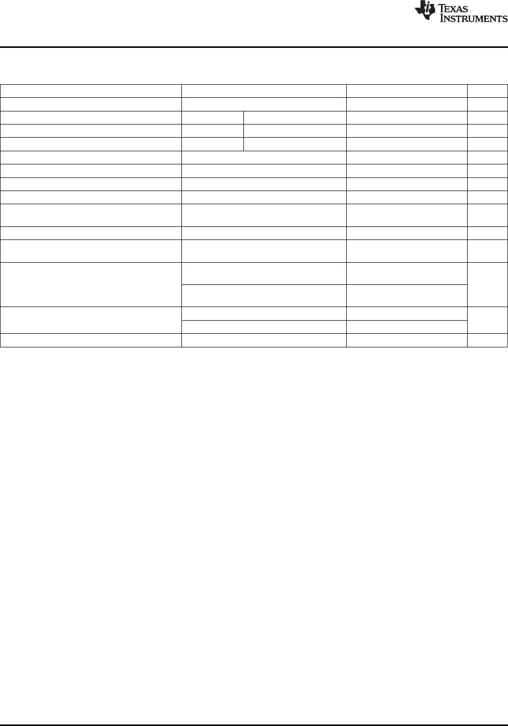
ELECTRICAL CHARACTERISTICS
T
A
= 25°C, VDD = 3.6 V (unless otherwise noted)
PARAMETER TEST CONDITIONS MIN TYP MAX UNIT
V
REG
VREG 1.84 V
|I
IL
| Digital input low current EN VDD = 5.5 V , VIN = 0 V 1 µA
|I
IH
| Digital input high current EN VDD = 5.5 V, VIN = VDD 3.5 µA
V
OL
Digital output low voltage SDA I
OL
= 4 mA 0.4 V
I
SD
Shut down current V
EN
= 0 V 1.75 4 µA
I
SB
Standby current V
EN
= 1.8 V, STANDBY = 1 1.9 5 µA
I
DDQ
Quiescent current V
EN
= 1.8 V, STANDBY = 0, no signal 0.6 1 mA
R
IN
Input impedance IN/TRIG to GND 100 kΩ
IN/TRIG Common-Mode Voltage (AC
V
CM-ANA
AC_Couple = 1 0.9 V
Coupled)
R
OUT-SD
Output impedance in shutdown OUT+ to GND, OUT- to GND 15 kΩ
Load impedance threshold for over-
R
L-SD
OUT+ to GND, OUT- to GND 4 Ω
current detection
Time from GO or external trigger command
0.7
to output signal
t
SU
Start-up time ms
Time from EN high to output signal
1.5
(PWM/Analog Modes)
Duty Cycle = 90%, LRA Mode, No Load 2.5 3.25
Average battery current during
I
BAT, AVG
mA
operation
Duty Cycle = 90%, ERM Mode, No Load 2.5 3.25
f
SW
PWM Output Frequency 19.5 20.5 21.5 kHz
4 Submit Documentation Feedback Copyright © 2012–2014, Texas Instruments Incorporated
Product Folder Links: DRV2605