Datasheet
Table Of Contents
- FEATURES
- APPLICATIONS
- DESCRIPTION
- PINOUT INFORMATION
- ABSOLUTE MAXIMUM RATINGS
- THERMAL INFORMATION
- RECOMMENDED OPERATING CONDITIONS
- ELECTRICAL CHARACTERISTICS
- TIMING REQUIREMENTS
- TYPICAL CHARACTERISTICS
- SYSTEM DIAGRAMS
- APPLICATION INFORMATION
- ECCENTRIC ROTATING MASS MOTORS (ERM)
- LINEAR RESONANCE ACTUATORS (LRA)
- AUTO-RESONANCE ENGINE FOR LRA
- OPEN LOOP OPERATION FOR LRA
- SMART LOOP ARCHITECTURE
- AUTO CALIBRATION
- WAVEFORM LIBRARIES
- WAVEFORM SEQUENCER
- LIBRARY PARAMETERIZATION
- REAL-TIME PLAYBACK (RTP) MODE
- MULTI-MODE INPUT PIN (IN/TRIG)
- DEVICE ENABLE
- CONSTANT VIBRATION STRENGTH
- EDGE RATE CONTROL
- CAPACITOR SELECTION
- MODES OF OPERATION
- BLOCK DIAGRAM
- GENERAL I2C OPERATION
- SINGLE-BYTE AND MULTIPLE-BYTE TRANSFERS
- SINGLE-BYTE WRITE
- MULTIPLE-BYTE WRITE AND INCREMENTAL MULTIPLE-BYTE WRITE
- SINGLE-BYTE READ
- MULTIPLE-BYTE READ
- REGISTER MAP
- DEVICE PROGRAMMING
- WAVEFORM LIBRARY EFFECTS LIST
- PCB LAYOUT RECOMMENDATIONS
- Revision History

DRV2605
www.ti.com
SLOS825B –DECEMBER 2012–REVISED JANUARY 2014
Waveform Sequencer (Address: 0x04 to 0x0B)
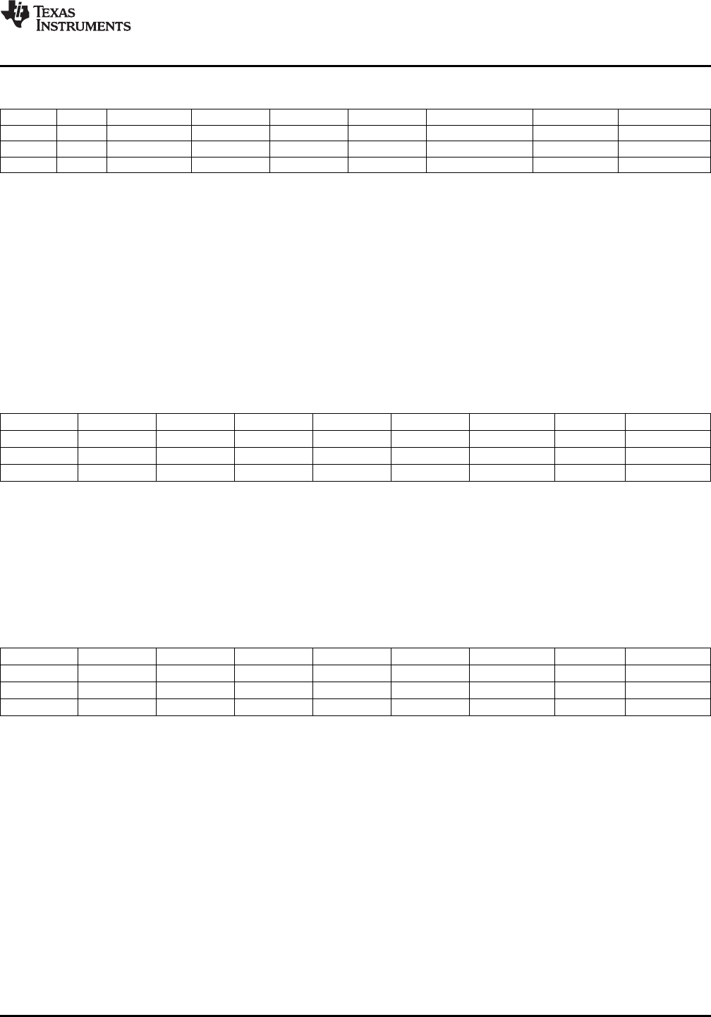
Bit 7 6 5 4 3 2 1 0
Function Wait WavfrmSeq[6] WavfrmSeq[5] WavfrmSeq[4] WavfrmSeq[3] WavfrmSeq[2] WavfrmSeq[1] WavfrmSeq[0]
Type R/W R/W R/W R/W R/W R/W R/W R/W
Default 0 0 0 0 0 0 0 0
Wait When this bit [7] is set, bits [6:0] are interpreted as a “wait time” in which the playback
engine will idle. This is used to insert timed delays between sequentially played waveforms.
Delay time is 10 ms * WavefrmSeq[6:0]. If Wait = 0, then WavfrmSeq[6:0] is interpreted as
a waveform identifier for sequence playback.
WavfrmSeq[6:0] Waveform Sequence value. Holds the waveform identifier of the waveform to be played. A
waveform identifier is an integer value referring to the index position of a waveform in a
ROM library. Playback begins at register address 0x04 when the user asserts the GO bit
(Register 0x0C). When playback of that waveform ends, the waveform sequencer plays the
next waveform identifier held in register 0x05, if it is non-zero. The waveform sequencer
continues in this fashion until it reaches an identifier value of zero, or all eight identifiers are
played (register addresses 0x04 through 0x0B), whichever comes first.
GO (Address: 0x0C)
Bit 7 6 5 4 3 2 1 0
Function GO
Type R/W
Default 0
GO Used to fire processes in the DRV2605. The process the GO bit fires is selected by the Mode[2:0] value
(Register 0x01). Its primary function is to fire playback of the waveform identifiers in the waveform
sequencer (Registers 0x04 to 0x0B), in which case, it can be thought of a “software trigger” for haptic
waveforms. The GO bit remains high until the playback of the haptic waveform sequence is complete.
Clearing the GO bit during waveform playback cancels the waveform sequence. Using one of the
external trigger modes can cause the GO bit to be set or cleared by the external trigger pin. It can also
be used to fire the auto calibration process or the diagnostic process.
OverDrive Time Offset (Address: 0x0D)
Bit 7 6 5 4 3 2 1 0
Function ODT[7] ODT[6] ODT[5] ODT[4] ODT[3] ODT[2] ODT[1] ODT[0]
Type R/W R/W R/W R/W R/W R/W R/W R/W
Default 0 0 0 0 0 0 0 0
ODT[7:0] Adds a time offset to the overdrive portion of the library waveforms. Some motors require more
overdrive time than others, so this register allows the user to add or take away overdrive time from
the library waveforms. The maximum voltage value in the library waveform is automatically
determined to be the overdrive portion. This register will only be useful in open loop mode.
Overdrive is automatic for closed loop mode. The offset is interpreted as two’s complement, so the
time offset may be positive or negative. OverDrive Time Offset (ms) = ODT[7:0] × 5
Copyright © 2012–2014, Texas Instruments Incorporated Submit Documentation Feedback 27
Product Folder Links: DRV2605


