
Datasheet


Table Of Contents
- FEATURES
- APPLICATIONS
- DESCRIPTION
- PINOUT INFORMATION
- ABSOLUTE MAXIMUM RATINGS
- THERMAL INFORMATION
- RECOMMENDED OPERATING CONDITIONS
- ELECTRICAL CHARACTERISTICS
- TIMING REQUIREMENTS
- TYPICAL CHARACTERISTICS
- SYSTEM DIAGRAMS
- APPLICATION INFORMATION
- ECCENTRIC ROTATING MASS MOTORS (ERM)
- LINEAR RESONANCE ACTUATORS (LRA)
- AUTO-RESONANCE ENGINE FOR LRA
- OPEN LOOP OPERATION FOR LRA
- SMART LOOP ARCHITECTURE
- AUTO CALIBRATION
- WAVEFORM LIBRARIES
- WAVEFORM SEQUENCER
- LIBRARY PARAMETERIZATION
- REAL-TIME PLAYBACK (RTP) MODE
- MULTI-MODE INPUT PIN (IN/TRIG)
- DEVICE ENABLE
- CONSTANT VIBRATION STRENGTH
- EDGE RATE CONTROL
- CAPACITOR SELECTION
- MODES OF OPERATION
- BLOCK DIAGRAM
- GENERAL I2C OPERATION
- SINGLE-BYTE AND MULTIPLE-BYTE TRANSFERS
- SINGLE-BYTE WRITE
- MULTIPLE-BYTE WRITE AND INCREMENTAL MULTIPLE-BYTE WRITE
- SINGLE-BYTE READ
- MULTIPLE-BYTE READ
- REGISTER MAP
- DEVICE PROGRAMMING
- WAVEFORM LIBRARY EFFECTS LIST
- PCB LAYOUT RECOMMENDATIONS
- Revision History
D7 D0 ACK
Stop
Condition
Acknowledge
I CDevice Addressand
Read/WriteBit
2
Subaddress LastDataByte
A6 A5 A1 A0 R/W ACK A7 A5 A1 A0 ACK D7 ACK
Start
Condition
Acknowledge Acknowledge Acknowledge
FirstDataByte
A4 A3A6
OtherDataBytes
ACK
Acknowledge
D0 D7 D0
T0482-01
A6 A5 A4 A3 A2 A1 A0
R/W
ACK A7 A6 A5 A4 A3 A2 A1 A0 ACK D7 D6 D5 D4 D3 D2 D1 D0 ACK
Start
Condition
Stop
Condition
Acknowledge Acknowledge Acknowledge
I CDevice Addressand
Read/WriteBit
2
Subaddress DataByte
T0481-01
DRV2605
www.ti.com
SLOS825B –DECEMBER 2012–REVISED JANUARY 2014
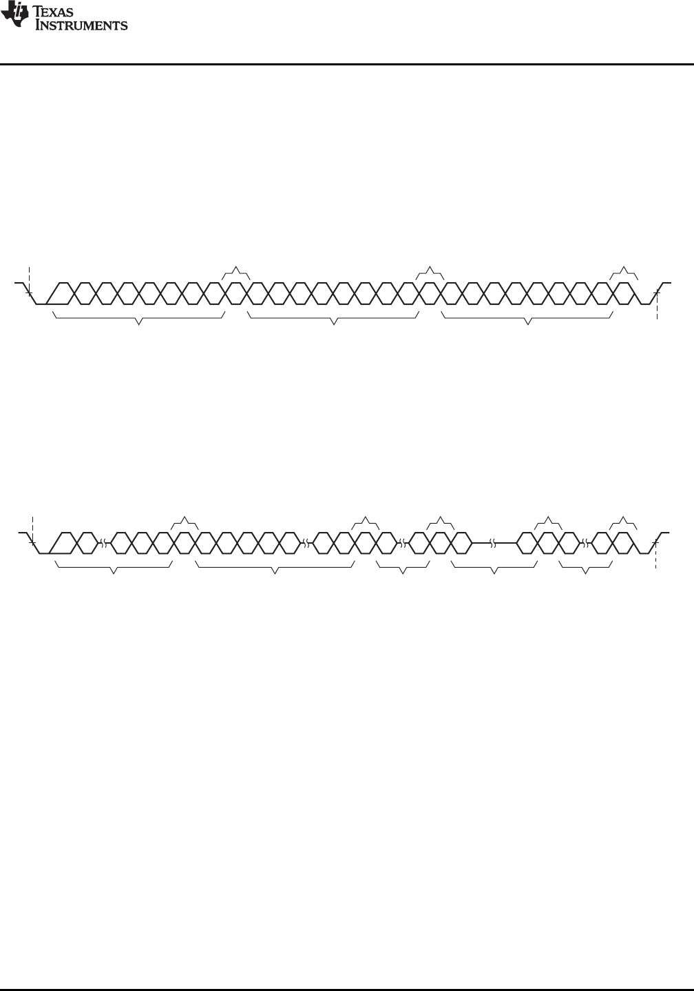
SINGLE-BYTE WRITE
As shown in Figure 20, a single-byte data-write transfer begins with the master device transmitting a start
condition followed by the I
2
C device address and the read/write bit. The read/write bit determines the direction of
the data transfer. For a write-data transfer, the read/write bit must be set to 0. After receiving the correct I
2
C
device address and the read/write bit, the DRV2605 responds with an acknowledge bit. Next, the master
transmits the register byte corresponding to theDRV2605 internal memory address being accessed. After
receiving the register byte, the DRV2605 again responds with an acknowledge bit. Finally, the master device
transmits a stop condition to complete the single-byte data-write transfer.
The DRV2605 address is 0x5A (7-bit), or 1011010 in binary.
Figure 20. Single-Byte Write Transfer
MULTIPLE-BYTE WRITE AND INCREMENTAL MULTIPLE-BYTE WRITE
A multiple-byte data write transfer is identical to a single-byte data write transfer except that multiple data bytes
are transmitted by the master device to the DRV2605 as shown in Figure 21. After receiving each data byte, the
DRV2605 responds with an acknowledge bit.
Figure 21. Multiple-Byte Write Transfer
Copyright © 2012–2014, Texas Instruments Incorporated Submit Documentation Feedback 21
Product Folder Links: DRV2605