
User manual

www.ti.com
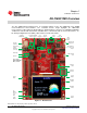
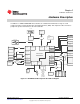
Functional Description
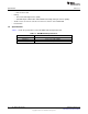
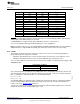
Table 2-1. JTAG Pin Table
JTAG (J1) Pin GPIO Pin (U1) Pin Functions Jumper J3 Pins
4 PC0 TCK 5, 6
2 PC1 TMS 3, 4
8 PC2 TDI 9, 10
6 PC3 TDO 7, 8
16 PA0 U0RX 13, 14
14 PA1 U0TX 15, 16
10 RESET 11, 12
18 TRST N/A
1 3.3V (with shunt) 1, 2
3, 11, 15, 17, 19 GND N/A
9 T_DISCONNECT 19, 20
5 EXTDBG (with shunt) 17, 18
12, 20 Reserved
EXTDBG is a signal that gets pulled low when attached to an external debugger. When pulled low, the
JTAG outputs of the ICDI controller are Z-stated.
T_DISCONNECT is a signal used to tell the ICDI when a device is connected to it.
J2 is a reserved jumper that may add functionality later. Leave unpopulated.
Note: The 20-pin connector (J1) is the ARM standard JTAG with ETM functionality connector. While the
TM4C129X devices support ETM functionality, this board does not have the necessary circuitry.
2.1.5 Power
The board is designed to be powered from one of two sources, they are selected by populating J11
jumper differently. The settings are as follows:
• Setting the shunt between pins 1 and 2 selects the barrel connector (J15) as the main 5-V source.
• Setting the shunt between pins 2 and 3 selects the ICDI USB (J4) as the power source.
J15 is a 6.5-mm diameter center power barrel connector. An example of a functional power supply is CUI
EMSA05300-P6P.
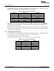
Power Jumper (J11) Options
Shunt on pin 1 and 2 Shunt on pin 2 and 3
Powered by J15 Powered by J4
The current and power consumption of the TM4C129X can be calculated by removing the shunt on J14
and measuring the voltage over the two pins, which are connected by a 1-Ω series resistor between the
pins. To calculate the current and power, use the following formulas:
I
TM4C129X
= V
J14
/ 1Ω (1)
P
TM4C129X
= V
J14
2
/ 1Ω (2)
The TPS62177DQC (U7) switching power regulator has many functions that are configured by omitting
resistors and including feedback to change the voltage on the 3.3-V rail. To learn more about these
features refer to the TPS62177DQC data sheet.
To power the external 3.3-V power supply without using the onboard voltage regulator (U7), remove the
shunt from J8 and connect 3.3-V directly to pin 1 of J8.
9
SPMU360–October 2013 Hardware Description
Submit Documentation Feedback
Copyright © 2013, Texas Instruments Incorporated