
User manual
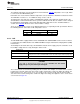

J27 J28
1 2
31 32
1 2
31 32
0.50
0.10
www.ti.com
Functional Description
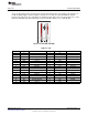
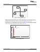
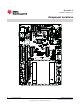
2.1.8.3 ULPI, MII, RMII, and EPI
There are two 16x2 headers on the left side of the board (J28 and J27). The majority of the J28 pins are
for MII and RMII signals, and the majority of J27 pins are for ULPI (an external USB PHY). Shared
between J28 and J27 are the connections for an EPI (host bus 16/8). There are also ground, +5V, +3.3V,
Hibernate and Wake pins mixed in with the connectors. Both headers are on a 100 mil grid.
Figure 2-4. ULPI, MII, and RMII
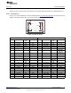
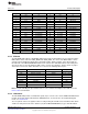
Table 2-4. J28
PIN PORT FUNCTION PIN PORT FUNCTION
1 5V 2 NC
3 PM6 EN0CRS 4 PF3 EN0MDIO
5 PF2 EN0MDC 6 PG7 EN0RXDV
7 PG2 EN0TXCLK 8 PA6 EN0RXCK/EPI0S8
9 GND Ground 10 GND
11 PM4 EN0RREFCLK 12 PN6 EN0TXER
13 PP0 EN0INTRN 14 3.3V
15 PQ5 EN0RXD0 16 PG3 EN0TXEN
17 PQ6 EN0RXD1 18 PG6 EN0RXER
19 PK5 EN0RXD2/EPI0S31/EN0LED2 20 PH0 EPI0S00
21 PK4 EN0RXD3/EPI0S32/EN0LED0 22 PH1 EPI0S01
23 PG4 EN0TXD0 24 PH2 EPI0S02
25 PG5 EN0TXD1 26 PH3 EPI0S03
27 PK6 EN0TXD2/EPI0S25/EN0LED1 28 PC7 EPI0S04
29 PK7 EN0TXD3/EPI0S24 30 PM7 EN0COL
31 GND Ground 32 GND
13
SPMU360–October 2013 Hardware Description
Submit Documentation Feedback
Copyright © 2013, Texas Instruments Incorporated