Tiva™ TM4C129X Development Board User's Guide Literature Number: SPMU360 October 2013
Contents 1 DK-TM4C129X Overview 1.1 1.2 1.3 1.4 2 Hardware Description 2.1 3 ...................................................................................................... 4 Kit Contents .................................................................................................................. Using the DK-TM4C129X .................................................................................................. Features ..................................................................
www.ti.com List of Figures 1-1. Board Picture ................................................................................................................ 4 2-1. DK-TM4C129X Development Board Block Diagram ................................................................... 7 2-2. Booster Pack 1............................................................................................................. 11 2-3. Booster Pack 2......................................................................
Chapter 1 SPMU360 – October 2013 DK-TM4C129X Overview The Tiva TM4C129X development kit is an evaluation platform for the Tiva TM4C129x-series ARM® Cortex™-M4-based microcontrollers. The evaluation board's design highlights the TM4C129X microcontroller's USB 2.0 On-The-Go/Host/Device (OTG/Host/Device) interface, the 10BASE-T/100BASETX Ethernet controller with internal PHY, QuadSSI bus to communicate with an external flash device, 12bit Analog-to-Digital Converter (ADC), LCD controller, and the I2C module.
Kit Contents www.ti.com 1.
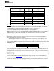
Specifications • • • 1.4 www.ti.com – RMII and MII external Ethernet PHY – EPI, Host bus 16/8 Debug – Tiva In-Circuit Debug Interface (ICDI) – Standard 20-pin JTAG header without ETM functionality (debug in and out capable) Shunt resistors to measure current on VDDVBATVDDA and VREF to the TM4C129X Reset button Specifications Table 1-1 shows the specifications for the DK-TM4C129X development board. Table 1-1. DK-TM4C129X Specifications Parameter 6 Value Board supply voltage 4.75-5.
Chapter 2 SPMU360 – October 2013 Hardware Description In addition to a TM4C129XNCZAD microcontroller, the evaluation board includes a range of useful peripheral features and an integrated in-circuit debug interface (ICDI). This chapter describes how these peripherals operate and interface to the microcontroller.
Functional Description 2.1 www.ti.com Functional Description 2.1.1 Microcontroller The Tiva TM4C129XNCZAD is an ARM® Cortex™-M4-based microcontroller with 1024-KB flash memory, 256-KB SRAM, 120-MHz operation, USB Host/Device/OTG, Ethernet Controller, Intergrated Ethernet PHY, Hibernation module, and a wide range of other peripherals. See the TM4C129XNCZAD microcontroller data sheet for complete device details. Most of the microcontroller signals are routed to 0.
Functional Description www.ti.com Table 2-1. JTAG Pin Table JTAG (J1) Pin GPIO Pin (U1) Pin Functions Jumper J3 Pins 4 PC0 TCK 5, 6 2 PC1 TMS 3, 4 8 PC2 TDI 9, 10 6 PC3 TDO 7, 8 16 PA0 U0RX 13, 14 14 PA1 U0TX 15, 16 10 RESET 11, 12 18 TRST N/A 1, 2 1 3.3V (with shunt) 3, 11, 15, 17, 19 GND N/A 9 T_DISCONNECT 19, 20 5 EXTDBG (with shunt) 17, 18 12, 20 Reserved EXTDBG is a signal that gets pulled low when attached to an external debugger.
Functional Description www.ti.com 2.1.6 USB Host/Device/OTG The DK-TM4C129X includes a USB Micro-AB (OTG) connector (J24) to allow for USB Host, Device, and OTG operation. Table 2-2 shows the signals that are used for USB OTG: Table 2-2.
Functional Description www.ti.com 2.1.8 Headers The three main sets of headers on the board are on a 0.100" grid and separated for a particular function. 2.1.8.1 BoosterPack 1 Figure 2-2 is a BoosterPack XL connection defined in the BoosterPack Design Guide. The port names and voltage rails are listed in the silk screen next to the pin of the header. AC D B 1 0.10 0.90 0.10 10 1.80 Figure 2-2.
Functional Description 2.1.8.2 www.ti.com BoosterPack 2 Figure 2-3 is a standard 20-pin BoosterPack (defined in the BoosterPack Design Guide). The port name, functionality, and voltage rail are printed on the silk screen near the pin. For the BoosterPack 2 UART port, the following jumpers must be set: J10 and J12 must have the shunts moved to pins 2 and 3 (this is the side that says BOOSTER2 UART).
Functional Description www.ti.com 2.1.8.3 ULPI, MII, RMII, and EPI There are two 16x2 headers on the left side of the board (J28 and J27). The majority of the J28 pins are for MII and RMII signals, and the majority of J27 pins are for ULPI (an external USB PHY). Shared between J28 and J27 are the connections for an EPI (host bus 16/8). There are also ground, +5V, +3.3V, Hibernate and Wake pins mixed in with the connectors. Both headers are on a 100 mil grid. J27 1 J28 2 1 2 0.10 31 32 31 32 0.
Functional Description www.ti.com Table 2-5. J27 PIN PORT 1 5V 3 PB3 5 GND 7 PL1 9 PL0 11 FUNCTION PIN PORT 2 NC USB0CLK/EPI0S28/EN0MDIO FUNCTION 4 NC 6 3.
Functional Description www.ti.com 2.1.11 Temperature Sensor The ambient temperature is measured by the Texas Instruments TMP100 temperature sensor (U4), which is connected to the TM4C129X by I2C. I2C module 6 is used to interface with the temperature sensor, which has a maximum resolution of 12 bits. The TMP100 is accurate to +/- 2 °C within the range of -25 to +85 °C. The initial value of the I2C slave address is 0b1001010 or 0x4A, code required to configure them.
Functional Description www.ti.com PT3/YD PT2/XL PE7/XR PP7/YU Figure 2-5. Resistive Touch Screen Note: The analog input PE7 (AIN21) is under commit control and extra steps are required in software to enable the function of the pin to be changed, see the "Commit Control" section of the datasheet for more information and the software steps required to enable proper operation of the touch screen. J34 enables the use of another display or other uses of the LCD pins.
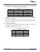
Functional Description www.ti.com Table 2-6. J34 PIN PORT FUNCTION PIN LCD PIN NAME 1 3 LCD FUNCTION N/A 5V 2 N/A 5V N/A 3.3V 4 N/A 3.
Chapter 3 SPMU360 – October 2013 Software Development This chapter provides general information on software development as well as instructions for flash memory programming. 3.1 Software Description The software provided with the DK-TM4C129X provides access to all of the peripheral devices supplied in the design. The TivaWare™ for C Series Peripheral Driver Library is used to operate the on-chip peripherals.
Programming the DK-TM4C129X Board www.ti.com 1. Install the Stellaris ICDI drivers on a Windows PC. Refer to the README First and the Stellaris Driver Installation Guide. 2. Install LM Flash Programmer on the PC. 3. Connect the USB-A cable plug to an available port on the PC and the Mini-B plug to the board. 4. Verify that the power LEDs (D9, D10 and D1) on the board are lit. 5. Run LM Flash Programmer. 6. In the Configuration tab, use the Quick Set control to select the DK-TM4C129X development board. 7.
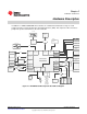
Appendix A SPMU360 – October 2013 Component Locations Figure A-1.
Appendix A www.ti.com Figure A-2.
Appendix A www.ti.com Figure A-3.
Appendix B SPMU360 – October 2013 Bill of Materials (BOM) Item Ref Qty Description Mfg Part Number TDK C1608X7R1H332K 1 C1, C30 2 Capacitor, 3300pF, 50V, 10%, X7R, 0603 2 C12, C55 2 Capacitor, 2.2uF, 16V, 10%, 0603, X5R Murata GRM188R61C225KE15D 34 Capacitor, 0.
Appendix B 24 www.ti.com Item Ref Qty Description Mfg Part Number 23 D13 1 Diode, Schottky, 60V, 15ma, SOD-323 Diodes Inc SD101AWS-7-F 24 D14 1 Diode, 8 chan, +/-15KV, ESD Protection Array, SO-8 Semtech SLVU2.8-4.TBT 25 D16 1 LED, Red 630nm, Clear 0805 SMD Lite-On LTST-C171EKT 26 D3, D4, D5, D6, D7 5 Diode, 5.6V ESD Suppressor 0402 EPCOS B72590D0050H160 27 D8, D9 2 LED AMBER CLEAR 0805 SMD Lite-On LTST-C170AKT 28 J1 1 Header, 2x10, 2.
Appendix B www.ti.com Item Ref Qty Description Mfg Part Number 49 L2 1 Inductor 6.8uH, SMD 4mmx4mm, 1.06A, 0.132 Ohm Taiyo Yuden NR4018T6R8M 50 Q1, Q2, Q3, Q4 4 NPN SC70 pre-biased Diodes Inc DTC114EET1G Panasonic ERJ-3GEYJ104V 51 R1 1 Resistor, 100K OHM 1/10W 5% 0603 Thick 52 R14 1 Resistor, 1K Ohm, 1/10W, 5%, SMD, Thick Panasonic ERJ-3GEYJ102V 53 R18 1 Resistor, 5.
Appendix B www.ti.com Item Ref Qty Description Mfg Part Number 78 U4 1 IC, Digital Temperature Sensor -55C to +125C, +/-3C, SOT23-6 Texas Instruments TMP100NA 79 U5 1 Load Switch, 5.5V, SOT23-5, TPS2051BDBV Texas Instruments TPS2051BDBVT 80 U6 1 Op Amp, 0.35W AUDIO MONO AB, 8TSSOP Texas Instruments LM4819MM 81 U7 1 Regulator, Step Down 3.3V, 0.5A Texas Instruments TPS62177DQC 82 U8 1 Precision 3.
Appendix C SPMU360 – October 2013 References In addition to this document, the following references are included on the Tiva TM4C123GH6PGE Development Kit USB flash drive and are also available for download at www.ti.com.
Appendix D SPMU360 – October 2013 Schematics This section contains the schematics for the DK-TM4C129X board. • Microcontroller, crystals and decoupling capacitors, page 1 • Ethernet, USB, and MII/RMII, ULPI and EPI headers, page 2 • SD card solt, SPI flash, temperature sensor, and speaker with amplifier, page 3 • BoosterPack headers and EM connectors, page 4 • LCD backlight driver, VREF regulator, 3.
3.3V 3.
LED2 NOTE: Pull up resistors and decoupling cap should be located near U1 1 3 5 PK4/EN0RXD3/LED0 PK6/EN0TXD2/LED1 PF1/LED2 J33 LED1 LED0 LED1 LED2 SPEED(AMBER) 330 Amber 3.3V 3.3V 2 4 6 R45 D8 D15 R47 330 ACTIVITY(GREEN) R46 330 LINK(RED) Green CON-HDR-2X3-0100 C65 C62 0.1uF R42 R41 R40 LED0 0.1uF R37 D16 RED 3.3V 49.9 U1-C EN0TXOP V15 EN0TX+ 49.9 49.9 49.9 T1 3.3V EN0TXON P17 N16 EN0RXIP VDD VDD R17 P16 V14 EN0TXW13 EN0RX+ 3.
3.3V_MAIN 3.3V_MAIN R5 +5V CS SIO1 SIO2 GND VCC SIO3 SCLK SIO0 8 7 6 5 U6 C14 J21 R26 PB2/USB0STP J7 FLASH_BUS 1 3 5 7 9 11 13 20K 0.047uF 2 4 6 8 10 12 14 3.3V_MAIN FLASH_CLK FLASH_DAT0 FLASH_DAT1 FLASH_DAT2 FLASH_DAT3 SD_CS 3.3V_MAIN J5 R59 10K microSD CARD INTERFACE CON-HDR-100-2X7-TH 3.3V_MAIN NC1 CS DI VDD CLK VSS DO RSV VO- VDD/2 BYPASS SD 5 2 8 1 VO+ + GND K1 R32 10K C51 0.1UF C J22 PD4/T3CCP0 Q1 DTC114EET1G B 9 10 11 12 R58 10K -IN +IN 0.
3.3V_MAIN +5V 3.3V_MAIN A A1 A2 A3 A4 A5 A6 A7 A8 A9 A10 PE2/AIN01 PH6/U5RX PH7/U5TX PN7 PF3/SSI3CLK PG7/SSI2CLK PJ2 PB4 PJ7 C1 C2 C3 C4 C5 C6 C7 C8 C9 C10 C71 PE3/AIN00 PE6/AIN20 PK0/AIN16 PK1/AIN17 PK2/AIN18 PK3/AIN19 PE0/AIN03 PE1/AIN02 C D EM_TX EM_RX PB7/I2C6SDA PB6/I2C6SCL +5V C72 B1 B2 B3 B4 B5 B6 B7 B8 B9 B10 J19 1uF PJ4/U3RTS 32K J30 PM5/T4CCP1 PD3/T1CCP1 PS3/T3CCP1 PL5/T0CCP1/USB0D5/EPI0S33 PL4/T0CCP0/USB0D4 PS0/T2CCP0 PS1/T2CCP1 PQ3/T7CCP1 PD2/T1CCP0 PM7/T5CCP1/EN0COL C77 0.
+5V ILED+ L2 IND-NR4018T 3.3V D11 C43 4.7uF U9 3 5 6 4 J35 1 2 FYV0704SMTF C41 8 7 1 2 VIN SW CTRL OVP GND LED FB RS 3.3V TL1 C42 0.1UF R43 10K 1uF U8 1 2 3 ILED- GND_F GND_S EN 3 3POS-HEADER V_OUT OUT_S V_IN 6 5 4 REF3230 TPS61042 9 PAD TL5 PF1/LED2 3 2 3.0_VREF+ TL4 1 6.8uH R52 10K C36 C35 0.1uF 0.1uF R50 13 3.3V_MAIN +5V Current Measure SW 2 VIN 2.2uF 50V R2 2.
3.3V_MAIN 3.3V_MAIN 3.3V_MAIN 3.3V_MAIN SW1 ILED+ ILED- +5V D10 D9 R48 10K SW2 2 4 6 SW3 CON-HDR-2X3-0100 SW4 3.3V_MAIN R57 C C85 C83 1uF 0.1uF TOUCH_AN0 TOUCH1 TOUCH0 TOUCH_AN1 LCDCLK LCDAC LCDDATA00 LCDDATA01 LCDDATA02 LCDDATA03 LCDDATA04 LCDDATA05 LCDDATA06 LCDDATA07 LCDFP LCDCP LCDLP LCDBUS C87 C86 1uF 0.1uF 1 3 5 7 9 11 13 15 17 19 21 23 25 27 29 31 33 35 37 39 2 4 6 8 10 12 14 16 18 20 22 24 26 28 30 32 34 36 38 40 R62 10K HDR-2X20-0100 330 3.
+ICDI_VBUS TARGET_DEBUG/COMM U3-A EXTDBG 3.3V_MAIN R11 10K 52 51 50 49 16 15 14 13 3.
EVALUATION BOARD/KIT/MODULE (EVM) ADDITIONAL TERMS Texas Instruments (TI) provides the enclosed Evaluation Board/Kit/Module (EVM) under the following conditions: The user assumes all responsibility and liability for proper and safe handling of the goods. Further, the user indemnifies TI from all claims arising from the handling or use of the goods.
FCC Interference Statement for Class B EVM devices This equipment has been tested and found to comply with the limits for a Class B digital device, pursuant to part 15 of the FCC Rules. These limits are designed to provide reasonable protection against harmful interference in a residential installation. This equipment generates, uses and can radiate radio frequency energy and, if not installed and used in accordance with the instructions, may cause harmful interference to radio communications.
【Important Notice for Users of EVMs for RF Products in Japan】 】 This development kit is NOT certified as Confirming to Technical Regulations of Radio Law of Japan If you use this product in Japan, you are required by Radio Law of Japan to follow the instructions below with respect to this product: 1. 2. 3. Use this product in a shielded room or any other test facility as defined in the notification #173 issued by Ministry of Internal Affairs and Communications on March 28, 2006, based on Sub-section 1.
EVALUATION BOARD/KIT/MODULE (EVM) WARNINGS, RESTRICTIONS AND DISCLAIMERS For Feasibility Evaluation Only, in Laboratory/Development Environments. Unless otherwise indicated, this EVM is not a finished electrical equipment and not intended for consumer use.
IMPORTANT NOTICE Texas Instruments Incorporated and its subsidiaries (TI) reserve the right to make corrections, enhancements, improvements and other changes to its semiconductor products and services per JESD46, latest issue, and to discontinue any product or service per JESD48, latest issue. Buyers should obtain the latest relevant information before placing orders and should verify that such information is current and complete.