
Network Router User Manual

SM320F2812-HT
www.ti.com
SGUS062A–JUNE 2009–REVISED APRIL 2010
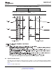
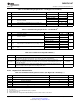
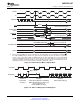
Table 6-5. XCLKIN Timing Requirements – PLL Bypassed or Enabled
(1)
NO. MIN MAX UNIT
C8 t
c(CI)
Cycle time, XCLKIN 6.67 250 ns
Up to 30 MHz 6
C9 t
f(CI)
Fall time, XCLKIN ns
30 MHz to 150 MHz 2
Up to 30 MHz 6
C10 t
r(CI)
Rise time, XCLKIN ns
30 MHz to 150 MHz 2
C11 t
w(CIL)
Pulse duration, X1/XCLKIN low as a percentage of t
c(CI)
40 60 %
C12 t
w(CIH)
Pulse duration, X1/XCLKIN high as a percentage of t
c(CI)
40 60 %
(1) Not production tested.
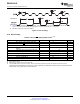
Table 6-6. XCLKIN Timing Requirements – PLL Disabled
(1)
NO. MIN MAX UNIT
C8 t
c(CI)
Cycle time, XCLKIN 6.67 250 ns
Up to 30 MHz 6
C9 t
f(CI)
Fall time, XCLKIN ns
30 MHz to 150 MHz 2
Up to 30 MHz 6
C10 t
r(CI)
Rise time, XCLKIN ns
30 MHz to 150 MHz 2
XCLKIN ≤ 120 MHz 40 60
C11 t
w(CIL)
Pulse duration, X1/XCLKIN low as a percentage of t
c(CI)
%
120 < XCLKIN ≤ 150 MHz 45 55
XCLKIN ≤ 120 MHz 40 60
Pulse duration, X1/XCLKIN high as a percentage of
C12 t
w(CIH)
%
t
c(CI)
120 < XCLKIN ≤ 150 MHz 45 55
(1) Not production tested.
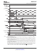
Table 6-7. Possible PLL Configuration Modes
(1)
PLL MODE REMARKS SYSCLKOUT
Invoked by tying XPLLDIS pin low upon reset. PLL block is completely disabled. Clock input to the
PLL Disabled XCLKIN
CPU (CLKIN) is directly derived from the clock signal present at the X1/XCLKIN pin.
Default PLL configuration upon power-up, if PLL is not disabled. The PLL itself is bypassed.
PLL Bypassed However, the /2 module in the PLL block divides the clock input at the X1/XCLKIN pin by two before XCLKIN/2
feeding it to the CPU.
Achieved by writing a non-zero value n into PLLCR register. The /2 module in the PLL block now
PLL Enabled (XCLKIN × n)/2
divides the output of the PLL by two before feeding it to the CPU.
(1) Not production tested.
6.13.2 Output Clock Characteristics
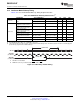
Table 6-8. XCLKOUT Switching Characteristics (PLL Bypassed or Enabled)
(1) (2)
NO. PARAMETER MIN TYP MAX UNIT
C1 t
c(XCO)
Cycle time, XCLKOUT 6.67
(3)
ns
C3
(4)
t
f(XCO)
Fall time, XCLKOUT 2 ns
C4
(4)
t
r(XCO)
Rise time, XCLKOUT 2 ns
C5
(4)
t
w(XCOL)
Pulse duration, XCLKOUT low H–2 H+2 ns
C6
(4)
t
w(XCOH)
Pulse duration, XCLKOUT high H–2 H+2 ns
C7
(4)
t
p
PLL lock time
(5)
131 072t
c(CI)
ns
(1) A load of 40 pF is assumed for these parameters.
(2) H = 0.5t
c(XCO)
(3) The PLL must be used for maximum frequency operation.
(4) Not production tested..
(5) This parameter has changed from 4096 XCLKIN cycles in the earlier revisions of the silicon.
Copyright © 2009–2010, Texas Instruments Incorporated Electrical Specifications 95
Submit Documentation Feedback
Product Folder Link(s): SM320F2812-HT