
Network Router User Manual
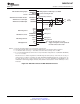
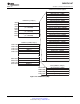

ADCINA[7:0]
ADCINB[7:0]
ADCLO
ADCBGREFIN
†
ADC External Current Bias Resistor ADCRESEXT
ADCREFP
V
DDA1
V
DDA2
V
SSA1
V
SSA2
AVDDREFBG
AVSSREFBG
V
DDAIO
V
SSAIO
V
DD1
V
SS1
Test Pin
ADC Reference Positive Output
ADCREFMADC Reference Medium Output
ADC Analog Power
ADC Reference Power
ADC Analog I/O Power
ADC Digital Power
Analog input 0−3 V with respect to ADCLO
Connect to Analog Ground
24.9 k/20 k (See Note C)
10 F
‡
10 F
‡
Analog 3.3 V
Analog 3.3 V
Analog 3.3 V
Analog 3.3 V
Analog Ground
1.8 V
ADCREFP and ADCREFM should not
be loaded by external circuitry
can use the same 1.8 V (or 1.9 V) supply as the
digital core but separate the two with a ferrite
bead or a filter
Digital Ground
ADC 16-Channel Analog Inputs
†
Provide access to this pin in PCB layouts. Intended for test purposes only.
‡
TAIYO YUDEN EMK325F106ZH, EMK325BJ106MD, or equivalent
NOTES: A. External decoupling capacitors are recommended on all power pins.
B. Analog inputs must be driven from an operational amplifier that does not degrade the ADC performance.
C. Use 24.9 kΩ for ADC clock range 1 − 18.75 MHz; use 20 kΩ for ADC clock range 18.75 − 25 MHz.
SM320F2812-HT
SGUS062A–JUNE 2009 –REVISED APRIL 2010
www.ti.com
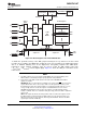
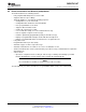
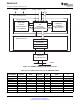
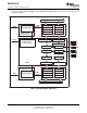
Figure 4-5 shows the ADC pin-biasing for internal reference and Figure 4-6 shows the ADC pin-biasing for
external reference.
Figure 4-5. ADC Pin Connections With Internal Reference (See Notes A and B)
NOTE
The temperature rating of any recommended component must match the rating of the end
product.
62 Peripherals Copyright © 2009–2010, Texas Instruments Incorporated
Submit Documentation Feedback
Product Folder Link(s): SM320F2812-HT