
Network Router User Manual

SM320F2812-HT
SGUS062A–JUNE 2009 –REVISED APRIL 2010
www.ti.com
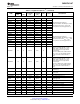
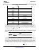
Table 2-3. Signal Descriptions
(1)
(continued)
PIN NO.
DIE PAD DIE PAD
DIE PAD
NAME X-CENTER Y-CENTER I/O/Z
(2)
PU/PD
(3)
DESCRIPTION
172-PIN
NO.
(mm) (mm)
HFG
POWER SIGNALS
V
DD
22 29 2927.6 42.6
V
DD
36 43 4395.4 42.6
V
DD
55 62 5361.5 1256.0
V
DD
73 86 5361.5 3496.4
1.8-V or 1.9-V Core Digital Power Pins. See
V
DD
- 98 5361.5 4671.835
Section 6.2, Recommended Operating
V
DD
98 113 3861.3 5057.5
Conditions, for voltage requirements.
V
DD
110 125 2451.9 5057.5
V
DD
125 141 663.7 5057.5
V
DD
140 156 42.6 3845.1
V
DD
150 169 42.6 2635.3
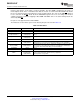
V
SS
- 25 2517.7 42.6
V
SS
31 38 3871.3 42.6
V
SS
37 44 4490.7 42.6
V
SS
51 58 5361.5 869.2
V
SS
57 65 5361.5 1514.6
V
SS
- 79 5361.5 2818.6
V
SS
76 89 5361.5 3754.9
V
SS
84 97 5361.5 4585.7
Core and Digital I/O Ground Pins
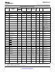
V
SS
97 112 3956.0 5057.5
V
SS
103 118 3280.5 5057.5
V
SS
111 126 2357.2 5057.5
V
SS
- 133 1587.1 5057.5
V
SS
126 142 569.0 5057.5
V
SS
139 155 42.6 3915.2
V
SS
- 159 42.6 3580.8
V
SS
- 168 42.6 2705.4
V
DDIO
30 37 3776.0 42.6
V
DDIO
63 73 5361.5 2226.0
V
DDIO
79 92 5361.5 4051.2
3.3–V I/O Digital Power Pins
V
DDIO
- 105 4784.7 5057.5
V
DDIO
112 127 2262.5 5057.5
V
DDIO
142 160 42.6 3510.7
3.3–V Flash Core Power Pin. This pin
should be connected to 3.3 V at all times
after power-up sequence requirements
V
DD3VFL
68 78 5361.5 2732.4
have been met. This pin is used as VDDIO
in ROM parts and must be connected to
3.3 V in ROM parts as well.
22 Introduction Copyright © 2009–2010, Texas Instruments Incorporated
Submit Documentation Feedback
Product Folder Link(s): SM320F2812-HT