
Network Router User Manual

SM320F2812-HT
www.ti.com
SGUS062A–JUNE 2009–REVISED APRIL 2010
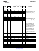
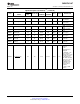
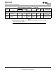
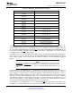
Table 2-3. Signal Descriptions
(1)
(continued)
PIN NO.
DIE PAD DIE PAD
DIE PAD
NAME X-CENTER Y-CENTER I/O/Z
(2)
PU/PD
(3)
DESCRIPTION
172-PIN
NO.
(mm) (mm)
HFG
ADC ANALOG INPUT SIGNALS
ADCINA7 163 186 42.6 1253.9 I
ADCINA6 164 188 42.6 1094.3 I
ADCINA5 165 190 42.6 954.0 I
Eight-channel analog inputs for
ADCINA4 166 192 42.6 794.4 I
Sample-and-Hold A. The ADC pins should
not be driven before V
DDA1
, V
DDA2
, and
ADCINA3 167 194 42.6 654.1 I
V
DDAIO
pins have been fully powered up.
ADCINA2 168 196 42.6 513.9 I
ADCINA1 169 197 42.6 434.1 I
ADCINA0 170 198 42.6 354.3 I
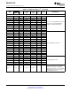
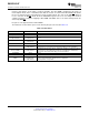
ADCINB7 9 13 1355.2 42.6 I
ADCINB6 8 11 1164.6 42.6 I
ADCINB5 7 10 1069.2 42.6 I
Eight-channel analog inputs for
ADCINB4 6 8 878.6 42.6 I
Sample-and-Hold B. The ADC pins should
not be driven before the V
DDA1
, V
DDA2
, and
ADCINB3 5 6 688.0 42.6 I
V
DDAIO
pins have been fully powered up.
ADCINB2 4 4 497.4 42.6 I
ADCINB1 3 3 402.1 42.6 I
ADCINB0 2 2 306.8 42.6 I
ADC Voltage Reference Output (2 V).
Requires a low ESR (50 mΩ – 1.5 Ω)
ceramic bypass capacitor of 10 mF to
analog ground. (Can accept external
ADCREFP 11 15 1545.8 42.6 O reference input
(2 V) if the software bit is enabled for this
mode. 1-mF to 10-mF low ESR capacitor
can be used in the external reference
mode.)
ADC Voltage Reference Output (1 V).
Requires a low ESR (50 mΩ – 1.5 Ω)
ceramic bypass capacitor of 10 mF to
analog ground. (Can accept external
ADCREFM 10 14 1450.5 42.6 O reference input
(1 V) if the software bit is enabled for this
mode. 1-mF to 10-mF low ESR capacitor
can be used in the external reference
mode.)
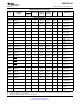
ADC External Current Bias Resistor
ADCRESEXT 16 22 2212.9 42.63 O
(24.9 kΩ ±5%)
Test Pin. Reserved for TI. Must be left
ADCBGREFIN 160 180 42.6 1680.9 I
unconnected.
AVSSREFBG 12 17 1831.7 42.6 I ADC Analog GND
AVDDREFBG 13 18 1736.4 42.6 I ADC Analog Power (3.3 V)
Common Low Side Analog Input. Connect
ADCLO 171 199 42.6 274.5 I
to analog ground.
V
SSA1
15 21 2117.6 42.6 I ADC Analog GND
V
SSA2
161 182 42.6 1550.7 I ADC Analog GND
V
DDA1
14 19 1927.0 42.6 I ADC Analog 3.3-V Supply
V
DDA2
162 184 42.6 1394.2 I ADC Analog 3.3-V Supply
V
SS1
159 178 42.6 1830.8 I ADC Digital GND
V
DD1
158 177 42.6 1901.0 I ADC Digital 1.8-V (or 1.9-V) Supply
V
DDAIO
1 1 211.5 42.6 3.3-V Analog I/O Power Pin
V
SSAIO
172 200 42.6 204.3 Analog I/O Ground Pin
Copyright © 2009–2010, Texas Instruments Incorporated Introduction 21
Submit Documentation Feedback
Product Folder Link(s): SM320F2812-HT