
Network Router User Manual

SM320F2812-HT
www.ti.com
SGUS062A–JUNE 2009–REVISED APRIL 2010
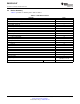
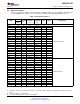
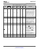
Table 2-3. Signal Descriptions
(1)
(continued)
PIN NO.
DIE PAD DIE PAD
DIE PAD
NAME X-CENTER Y-CENTER I/O/Z
(2)
PU/PD
(3)
DESCRIPTION
172-PIN
NO.
(mm) (mm)
HFG
JTAG AND MISCELLANEOUS SIGNALS
Oscillator Input – input to the internal
oscillator. This pin is also used to feed an
external clock. The 28× can be operated
with an external clock source, provided that
the proper voltage levels be driven on the
X1/XCLKIN pin. It should be noted that the
X1/XCLKIN pin is referenced to the 1.8-V
X1/XCLKIN 75 88 5361.5 3668.7 I
(or 1.9-V) core digital power supply (V
DD
),
rather than the 3.3-V I/O supply (V
DDIO
). A
clamping diode may be used to clamp a
buffered clock signal to ensure that the
logic-high level does not exceed V
DD
(1.8 V or 1.9 V) or a 1.8-V oscillator may be
used.
X2 74 87 5361.5 3582.6 O Oscillator Output
Output clock derived from SYSCLKOUT to
be used for external wait-state generation
and as a general-purpose clock source.
XCLKOUT is either the same frequency,
XCLKOUT 117 132 1701.2 5057.5 O – 1/2 the frequency, or 1/4 the frequency of
SYSCLKOUT. At reset, XCLKOUT =
SYSCLKOUT/4. The XCLKOUT signal can
be turned off by setting bit 3 (CLKOFF) of
the XINTCNF2 register to 1.
Test Pin. Reserved for TI. Must be
TESTSEL 131 147 42.6 4764.6 I PD
connected to ground.
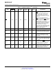
Device Reset (in) and Watchdog Reset
(out).
Device reset. XRS causes the device to
terminate execution. The PC points to the
address contained at the location
0x3FFFC0. When XRS is brought to a high
level, execution begins at the location
pointed to by the PC. This pin is driven low
XRS 156 175 42.6 2077.8 I/O PU
by the DSP when a watchdog reset occurs.
During watchdog reset, the XRS pin is
driven low for the watchdog reset duration
of 512 XCLKIN cycles.
The output buffer of this pin is an
open-drain with an internal pullup (100 mA,
typical). It is recommended that this pin be
driven by an open-drain device.
Test Pin. Reserved for TI. On F281x
TEST1 66 76 5361.5 2522.3 I/O –
devices, TEST1 must be left unconnected.
Test Pin. Reserved for TI. On F281x
TEST2 65 75 5361.5 2436.1 I/O –
devices, TEST2 must be left unconnected.
Copyright © 2009–2010, Texas Instruments Incorporated Introduction 19
Submit Documentation Feedback
Product Folder Link(s): SM320F2812-HT