
Network Router User Manual
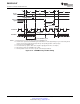
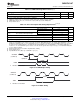
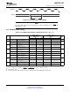

t
w(PWM)
t
d(PWM)XCO
PWMx
XCLKOUT
(see Note A)
XCLKOUT
(see Note A)
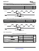
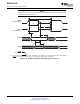
t
w(TDIR)
TDIRx
SM320F2812-HT
www.ti.com
SGUS062A–JUNE 2009–REVISED APRIL 2010
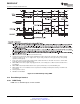
Table 6-13. PWM Switching Characteristics
(1) (2)
PARAMETER TEST CONDITIONS MIN MAX UNIT
t
w(PWM)
(3) (4)
Pulse duration, PWMx output high/low 25 ns
t
d(PWM)XCO
Delay time, XCLKOUT high to PWMx output switching XCLKOUT = SYSCLKOUT/4 10 ns
(1) See the GPIO output timing for fall/rise times for PWM pins.
(2) PWM pin toggling frequency is limited by the GPIO output buffer switching frequency (20 MHz).
(3) PWM outputs may be 100%, 0%, or increments of t
c(HCO)
with respect to the PWM period.
(4) Not production tested.
Table 6-14. Timer and Capture Unit Timing Requirements
(1) (2) (3)
MIN MAX UNIT
Without input qualifier 2 × t
c(SCO)
t
w(TDIR)
Pulse duration, TDIRx low/high cycles
With input qualifier 1 × t
c(SCO)
+ IQT
(4)
Without input qualifier 2 × t
c(SCO)
t
w(CAP)
Pulse duration, CAPx input low/high cycles
With input qualifier 1 x t
c(SCO)
+ IQT
(4)
t
w(TCLKINL)
Pulse duration, TCLKINx low as a percentage of TCLKINx cycle time 40 60 %
t
w(TCLKINH)
Pulse duration, TCLKINx high as a percentage of TCLKINx cycle time 40 60 %
t
c(TCLKIN)
Cycle time, TCLKINx 4 × t
c(HCO)
ns
(1) The QUALPRD bit field value can range from 0 (no qualification) through 0xFF (510 SYSCLKOUT cycles). The qualification sampling
period is 2n SYSCLKOUT cycles, where n is the value stored in the QUALPRD bit field. As an example, when QUALPRD = 1, the
qualification sampling period is 1 × 2 = 2 SYSCLKOUT cycles (i.e., the input is sampled every 2 SYSCLKOUT cycles). Six such samples
are taken over five sampling windows, each window being 2n SYSCLKOUT cycles. For QUALPRD = 1, the minimum width that is
needed is 5 × 2 = 10 SYSCLKOUT cycles. However, since the external signal is driven asynchronously, a 11-SYSCLKOUT-wide pulse
ensures reliable recognition.
(2) Maximum input frequency to the QEP = min[HSPCLK/2, 20 MHz]
(3) Not production tested.
(4) Input Qualification Time (IQT) = [5 × QUALPRD × 2] × t
c(SCO)
A. XCLKOUT = SYSCLKOUT
Figure 6-16. PWM Output Timing
A. XCLKOUT = SYSCLKOUT
Figure 6-17. TDIRx Timing
Copyright © 2009–2010, Texas Instruments Incorporated Electrical Specifications 105
Submit Documentation Feedback
Product Folder Link(s): SM320F2812-HT