
Evaluation Module User's Guide
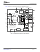

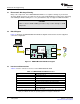

1.3 Functional Block Diagram
S
S
XTI
XTO
6.000MHz
96MHz
PLL(x16)
Tracker
(SpAct )
â
USBprotocol
controller
ISO-out
endpoint
Control
endpoint
ISO-in
endpoint
FIFO
FIFO
XCVR
Selector
Selector
Analog
PLL
Analog
PLL
USBSIE
V
REF
5Vto3.3V
Voltage
Regulator
Power
Manager
ADC
DAC
MIC
Bias
MIC
Amp
BGND V /V /V /V /V
CCA CCP CCL CCR DD
AGND/HGND/PGND/DGND
SSPND
V
BUS
D+
D-
POWER
MAMP
MMUTE
PLAY
REC
TEST0
TEST1
MBIAS
V
IN
V
COM2
V
COM1
V L
OUT
V R
OUT
FL
FR
PGA+30dBto
12dB
in1-dBsteps
-
ATT0dBto 76dB
in1-dBstepswithMute
-
ATT0dBto 76dB
in1-dBstepswithMute
-
HPAMP15mW(at32 )W
www.ti.com
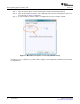
Functional Block Diagram
Figure 1-2 illustrates the functional block diagram of the DEM-PCM2912A EVM.
Figure 1-2. DEM-PCM2912A EVM Functional Block Diagram
SBAU141 – January 2009 Description 13
Submit Documentation Feedback