
Datasheet


DAC0830, DAC0832
www.ti.com
SNAS534B –MAY 1999–REVISED MARCH 2013
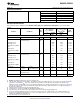
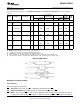
Electrical Characteristics
V
REF
=10.000 V
DC
unless otherwise noted. Boldface limits apply over temperature, T
MIN
≤T
A
≤T
MAX
.
(1)
For all other limits
T
A
=25°C.
V
CC
=12 V
DC
±5% V
CC
=5
V
CC
=15.75 V
DC
V
CC
=4.75 V
DC
to 15 V
DC
±5% V
DC
±5%
See Limit
Symbol Parameter Conditions
Note Units
Tested Tested Design
Typ
(2)
Design Limit
(4)
Typ
(2)
Limit
(3)
Limit
(3)
Limit
(4)
AC CHARACTERISTICS
(5)
t
s
Current Setting V
IL
=0V, V
IH
=5V
1.0 1.0 μs
Time
t
W
Write and XFER V
IL
=0V, V
IH
=5V See
(
100 250 375 600
5)
Pulse Width Min See
(
320 320 900 900
1)
t
DS
Data Setup Time V
IL
=0V, V
IH
=5V See
(
100 250 375 600
1)
Min 320 320 900 900
t
DH
Data Hold Time V
IL
=0V, V
IH
=5V See
(
30 50
ns
1)
Min 30 50
t
CS
Control Setup V
IL
=0V, V
IH
=5V See
(
110 250 600 900
Time
1)
Min 320 320 1100 1100
t
CH
Control Hold Time V
IL
=0V, V
IH
=5V See
(
0 0
0 10 0
1)
Min 0 0
(1) Boldface tested limits apply to the LJ and LCJ suffix parts only.
(2) Typicals are at 25°C and represent most likely parametric norm.
(3) Tested limits are ensured to TI's AOQL (Average Outgoing Quality Level).
(4) Ensured, but not 100% production tested. These limits are not used to calculate outgoing quality levels.
(5) The entire write pulse must occur within the valid data interval for the specified t
W
, t
DS
, t
DH
, and t
S
to apply.
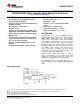
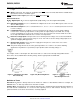
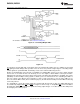
Switching Waveform
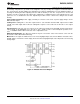
Definition of Package Pinouts
Control Signals
(All control signals level actuated)
CS: Chip Select (active low). The CS in combination with ILE will enable WR
1
.
ILE: Input Latch Enable (active high). The ILE in combination with CS enables WR
1
.
WR
1
: Write 1. The active low WR
1
is used to load the digital input data bits (DI) into the input latch. The data in
the input latch is latched when WR
1
is high. To update the input latch–CS and WR
1
must be low while ILE
Copyright © 1999–2013, Texas Instruments Incorporated Submit Documentation Feedback 5
Product Folder Links: DAC0830 DAC0832