
Datasheet


DAC0830, DAC0832
SNAS534B –MAY 1999–REVISED MARCH 2013
www.ti.com
Electrical Characteristics (continued)
V
REF
=10.000 V
DC
unless otherwise noted. Boldface limits apply over temperature, T
MIN
≤T
A
≤T
MAX
.
(1)
For all other limits
T
A
=25°C.
V
CC
= 5 V
DC
±5%
V
CC
= 4.75 V
DC
V
CC
= 12 V
DC
±5%
V
CC
= 15.75 V
DC
See Limit
to 15 V
DC
±5%
Parameter Conditions
Note Units
(2)
Tested Design
Typ
(3)
Limit
(4)
Limit
(5)
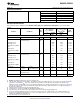
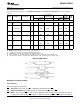
Power Supply Rejection All digital inputs latched high
V
CC
=14.5V to 15.5V 0.0002 0.0025 %
11.5V to 12.5V 0.0006 FSR/V
4.5V to 5.5V 0.013 0.015
Reference Max 15 20 20 kΩ
Input
Min 15 10 10 kΩ
Output Feedthrough Error V
REF
=20 Vp-p, f=100 kHz
3 mVp-p
All data inputs latched low
Output Leakage I
OUT1
All data inputs LJ & LCJ See
(8)
100 100
nA
Current Max
(8)
latched low LCN, LCWM & LCV 50 100
I
OUT2
All data inputs LJ & LCJ 100 100
nA
latched high LCN, LCWM & LCV 50 100
Output I
OUT1
All data inputs 45
pF
Capacitance
I
OUT2
latched low 115
I
OUT1
All data inputs 130
pF
I
OUT2
latched high 30
DIGITAL AND DC CHARACTERISTICS
Digital Input Max Logic Low LJ: 4.75V 0.6
Voltages
LJ: 15.75V 0.8
LCJ: 4.75V 0.7 V
DC
LCJ: 15.75V 0.8
LCN, LCWM, LCV 0.95 0.8
Min Logic High LJ & LCJ 2.0 2.0
V
DC
LCN, LCWM, LCV 1.9 2.0
Digital Input Max Digital inputs LJ & LCJ −50 −200 −200 μA
Currents <0.8V
LCN, LCWM, LCV −160 −200 μA
Digital LJ & LCJ 0.1 +10 +10 μA
inputs>2.0V
LCN, LCWM, LCV +8 +10
Supply Current Max LJ & LCJ 1.2 3.5 3.5 mA
Drain
LCN, LCWM, LCV 1.7 2.0
(8) A 100nA leakage current with R
fb
=20k and V
REF
=10V corresponds to a zero error of (100×10
−9
×20×10
3
)×100/10 which is 0.02% of FS.
4 Submit Documentation Feedback Copyright © 1999–2013, Texas Instruments Incorporated
Product Folder Links: DAC0830 DAC0832