
Datasheet

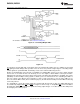

DAC0830, DAC0832
www.ti.com
SNAS534B –MAY 1999–REVISED MARCH 2013
Operating Conditions
Temperature Range T
MIN
≤T
A
≤T
MAX
Part numbers with “LCN” suffix 0°C to +70°C
Part numbers with “LCWM” suffix 0°C to +70°C
Part numbers with “LCV” suffix 0°C to +70°C
Part numbers with “LCJ” suffix −40°C to +85°C
Part numbers with “LJ” suffix −55°C to +125°C
Voltage at Any Digital Input V
CC
to GND
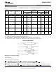
Electrical Characteristics
V
REF
=10.000 V
DC
unless otherwise noted. Boldface limits apply over temperature, T
MIN
≤T
A
≤T
MAX
.
(1)
For all other limits
T
A
=25°C.
V
CC
= 5 V
DC
±5%
V
CC
= 4.75 V
DC
V
CC
= 12 V
DC
±5%
V
CC
= 15.75 V
DC
See Limit
to 15 V
DC
±5%
Parameter Conditions
Note Units
(2)
Tested Design
Typ
(3)
Limit
(4)
Limit
(5)
CONVERTER CHARACTERISTICS
Resolution 8 8 8 bits
Linearity Error Max Zero and full scale adjusted See
(6)
−10V≤V
REF
≤+10V and
(2)
DAC0830LJ & LCJ 0.05 0.05 % FSR
DAC0832LJ & LCJ 0.2 0.2 % FSR
DAC0830LCN, LCWM & 0.05 0.05 % FSR
LCV
DAC0831LCN 0.1 0.1 % FSR
DAC0832LCN, LCWM & 0.2 0.2 % FSR
LCV
Differential Nonlinearity Zero and full scale adjusted See
(6)
Max −10V≤V
REF
≤+10V and
(2)
DAC0830LJ & LCJ 0.1 0.1 % FSR
DAC0832LJ & LCJ 0.4 0.4 % FSR
DAC0830LCN, LCWM & 0.1 0.1 % FSR
LCV
DAC0831LCN 0.2 0.2 % FSR
DAC0832LCN, LCWM & 0.4 0.4 % FSR
LCV
Monotonicity −10V≤V
REF
LJ & LCJ See
(6)
8 8 bits
≤+10V LCN, LCWM & LCV 8 8 bits
Gain Error Max Using Internal R
fb
See
(7)
±0.2 ±1 ±1 % FS
−10V≤V
REF
≤+10V
%
Gain Error Tempco Max Using internal R
fb
0.0002 0.0006
FS/°C
(1) Boldface tested limits apply to the LJ and LCJ suffix parts only.
(2) The unit “FSR” stands for “Full Scale Range.” “Linearity Error” and “Power Supply Rejection” specs are based on this unit to eliminate
dependence on a particular V
REF
value and to indicate the true performance of the part. The “Linearity Error” specification of the
DAC0830 is “0.05% of FSR (MAX)”. This ensures that after performing a zero and full scale adjustment (see sections Zero Adjustment
and Full-Scale Adjustment), the plot of the 256 analog voltage outputs will each be within 0.05%×V
REF
of a straight line which passes
through zero and full scale.
(3) Typicals are at 25°C and represent most likely parametric norm.
(4) Tested limits are ensured to TI's AOQL (Average Outgoing Quality Level).
(5) Ensured, but not 100% production tested. These limits are not used to calculate outgoing quality levels.
(6) For current switching applications, both I
OUT1
and I
OUT2
must go to ground or the “Virtual Ground” of an operational amplifier. The
linearity error is degraded by approximately V
OS
÷ V
REF
. For example, if V
REF
= 10V then a 1 mV offset, V
OS
, on I
OUT1
or I
OUT2
will
introduce an additional 0.01% linearity error.
(7) Specified at V
REF
=±10 V
DC
and V
REF
=±1 V
DC
.
Copyright © 1999–2013, Texas Instruments Incorporated Submit Documentation Feedback 3
Product Folder Links: DAC0830 DAC0832