
Datasheet


DAC0830, DAC0832
www.ti.com
SNAS534B –MAY 1999–REVISED MARCH 2013
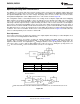
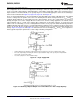
Input Code IDEAL V
OUT
MSB LSB +V
REF
−V
REF
1 1 1 1 1 1 1 1
1 1 0 0 0 0 0 0
1 0 0 0 0 0 0 0
0 1 1 1 1 1 1 1
0 0 1 1 1 1 1 1
0 0 0 0 0 0 0 0
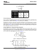
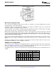
Full-Scale Adjustment
In the case where the matching of R
fb
to the R value of the R-2R ladder (typically ±0.2%) is insufficient for full-
scale accuracy in a particular application, the V
REF
voltage can be adjusted or an external resistor and
potentiometer can be added as shown in Figure 21 to provide a full-scale adjustment.
The temperature coefficients of the resistors used for this adjustment are of an important concern. To prevent
degradation of the gain error temperature coefficient by the external resistors, their temperature coefficients
ideally would have to match that of the internal DAC resistors, which is a highly impractical constraint. For the
values shown in Figure 21, if the resistor and the potentiometer each had a temperature coefficient of ±100
ppm/°C maximum, the overall gain error temperature coefficent would be degraded a maximum of 0.0025%/°C
for an adjustment pot setting of less than 3% of R
fb
.
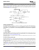
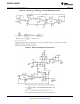
Using the DAC0830 in a Voltage Switching Configuration
The R-2R ladder can also be operated as a voltage switching network. In this mode the ladder is used in an
inverted manner from the standard current switching configuration. The reference voltage is connected to one of
the current output terminals (I
OUT1
for true binary digital control, I
OUT2
is for complementary binary) and the output
voltage is taken from the normal V
REF
pin. The converter output is now a voltage in the range from 0V to 255/256
V
REF
as a function of the applied digital code as shown in Figure 22.
Figure 21. Adding Full-Scale Adjustment
Figure 22. Voltage Mode Switching
Copyright © 1999–2013, Texas Instruments Incorporated Submit Documentation Feedback 15
Product Folder Links: DAC0830 DAC0832