
Datasheet


DAC0830, DAC0832
SNAS534B –MAY 1999–REVISED MARCH 2013
www.ti.com
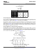
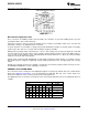
Bipolar Output Voltage with a Fixed Reference
The addition of a second op amp to the previous circuitry can be used to generate a bipolar output voltage from
a fixed reference voltage. This, in effect, gives sign significance to the MSB of the digital input word and allows
two-quadrant multiplication of the reference voltage. The polarity of the reference can also be reversed to realize
full 4-quadrant multiplication: ±V
REF
×±Digital Code=±V
OUT
. This circuit is shown in Figure 20.
This configuration features several improvements over existing circuits for bipolar outputs with other multiplying
DACs. Only the offset voltage of amplifier 1 has to be nulled to preserve linearity of the DAC. The offset voltage
error of the second op amp (although a constant output voltage error) has no effect on linearity. It should be
nulled only if absolute output accuracy is required. Finally, the values of the resistors around the second amplifier
do not have to match the internal DAC resistors, they need only to match and temperature track each other. A
thin film 4-resistor network available from Beckman Instruments, Inc. (part no. 694-3-R10K-D) is ideally suited for
this application. These resistors are matched to 0.1% and exhibit only 5 ppm/°C resistance tracking temperature
coefficient. Two of the four available 10 kΩ resistors can be paralleled to form R in Figure 20 and the other two
can be used independently as the resistances labeled 2R.
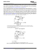
Zero Adjustment
For accurate conversions, the input offset voltage of the output amplifier must always be nulled. Amplifier offset
errors create an overall degradation of DAC linearity.
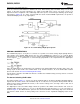
The fundamental purpose of zeroing is to make the voltage appearing at the DAC outputs as near 0V
DC
as
possible. This is accomplished for the typical DAC — op amp connection (Figure 18) by shorting out R
fb
, the
amplifier feedback resistor, and adjusting the V
OS
nulling potentiometer of the op amp until the output reads zero
volts. This is done, of course, with an applied digital code of all zeros if I
OUT1
is driving the op amp (all one's for
I
OUT2
). The short around R
fb
is then removed and the converter is zero adjusted.
Figure 19.
t
s
OP Amp C
C
(O to Full Scale)
LF356 22 pF 4 μs
LF351 22 pF 5 μs
LF357
(1)
10 pF 2 μs
(1) 2.4 kΩ RESISTOR ADDED FROM−INPUT TO GROUND TO
INSURE STABILITY
*THESE RESISTORS ARE AVAILABLE FROM BECKMAN INSTRUMENTS, INC. AS THEIR PART NO. 694-3-R10K-
D
Figure 20.
14 Submit Documentation Feedback Copyright © 1999–2013, Texas Instruments Incorporated
Product Folder Links: DAC0830 DAC0832