
Datasheet


DAC0830, DAC0832
www.ti.com
SNAS534B –MAY 1999–REVISED MARCH 2013
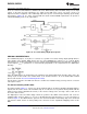
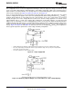
Basic Unipolar Output Voltage
To maintain linearity of output current with changes in the applied digital code, it is important that the voltages at
both of the current output pins be as near ground potential (0V
DC
) as possible. With V
REF
=+10V every millivolt
appearing at either I
OUT1
or I
OUT2
will cause a 0.01% linearity error. In most applications this output current is
converted to a voltage by using an op amp as shown in Figure 18.
The inverting input of the op amp is a “virtual ground” created by the feedback from its output through the internal
15 kΩ resistor, R
fb
. All of the output current (determined by the digital input and the reference voltage) will flow
through R
fb
to the output of the amplifier. Two-quadrant operation can be obtained by reversing the polarity of
V
REF
thus causing I
OUT1
to flow into the DAC and be sourced from the output of the amplifier. The output voltage,
in either case, is always equal to I
OUT1
×R
fb
and is the opposite polarity of the reference voltage.
The reference can be either a stable DC voltage source or an AC signal anywhere in the range from −10V to
+10V. The DAC can be thought of as a digitally controlled attenuator: the output voltage is always less than or
equal to the applied reference voltage. The V
REF
terminal of the device presents a nominal impedance of 15 kΩ
to ground to external circuitry.
Always use the internal R
fb
resistor to create an output voltage since this resistor matches (and tracks with
temperature) the value of the resistors used to generate the output current (I
OUT1
).
Figure 17.
Figure 18.
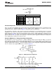
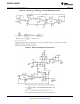
Op Amp Considerations
The op amp used in Figure 18 should have offset voltage nulling capability (See Section Zero Adjustment).
The selected op amp should have as low a value of input bias current as possible. The product of the bias
current times the feedback resistance creates an output voltage error which can be significant in low reference
voltage applications. BI-FET™ op amps are highly recommended for use with these DACs because of their very
low input current.
Transient response and settling time of the op amp are important in fast data throughput applications. The largest
stability problem is the feedback pole created by the feedback resistance, R
fb
, and the output capacitance of the
DAC. This appears from the op amp output to the (−) input and includes the stray capacitance at this node.
Addition of a lead capacitance, C
C
in Figure 19, greatly reduces overshoot and ringing at the output for a step
change in DAC output current.
Finally, the output voltage swing of the amplifier must be greater than V
REF
to allow reaching the full scale output
voltage. Depending on the loading on the output of the amplifier and the available op amp supply voltages (only
±12 volts in many development systems), a reference voltage less than 10 volts may be necessary to obtain the
full analog output voltage range.
Copyright © 1999–2013, Texas Instruments Incorporated Submit Documentation Feedback 13
Product Folder Links: DAC0830 DAC0832