
User manual

5.4 PLL Controller Register Map
www.ti.com
PLL Controller Register Map
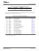
Table 5-3. PLL and Reset Controller Module Instance Table
Instance ID Base Address End Address Size
0 1C4 0800h 1C4 0BFFh 400h
1 1C4 0C00h 1C4 0FFFh 400h
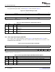
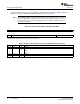
Table 5-4 lists the memory-mapped registers for the PLL and Reset Controller. See the device-specific
data manual for the memory address of these registers.
Table 5-4. PLL and Reset Controller Registers
Offset Acronym Register Description Section
00h PID Peripheral ID Register Section 5.4.1
E4h RSTYPE Reset Type Status Register Section 5.4.2
100h PLLCTL PLL Control Register Section 5.4.3
110h PLLM PLL Multiplier Control Register Section 5.4.4
118h PLLDIV1 PLL Controller Divider 1 Register Section 5.4.5
11Ch PLLDIV2
(1)
PLL Controller Divider 2 Register Section 5.4.6
120h PLLDIV3
(1)
PLL Controller Divider 3 Register Section 5.4.7
12Ch BPDIV
(1)
Bypass Divider Register Section 5.4.8
138h PLLCMD PLL Controller Command Register Section 5.4.9
13Ch PLLSTAT PLL Controller Status Register Section 5.4.10
140h ALNCTL PLL Controller Clock Align Control Register Section 5.4.11
144h DCHANGE PLLDIV Ratio Change Status Register Section 5.4.12
148h CKEN Clock Enable Control Register Section 5.4.13
14Ch CKSTAT Clock Status Register Section 5.4.14
150h SYSTAT SYSCLK Status Register Section 5.4.15
160h PLLDIV4
(1)
PLL Controller Divider 4 Register Section 5.4.16
164h PLLDIV5
(1)
PLL Controller Divider 5 Register Section 5.4.16
168h PLLDIV6
(1)
PLL Controller Divider 6 Register Section 5.4.16
170h PLLDIV8
(1)
PLL Controller Divider 8 Register Section 5.4.16
174h PLLDIV9
(1)
PLL Controller Divider 9 Register Section 5.4.16
(1)
For PLL1 only, not supported for PLL2
SPRUEP9A – May 2008 PLL Controller 45
Submit Documentation Feedback