
User manual

5.3.1 Device Clock Generation
5.3.2 Steps for Changing PLL2 Frequency
5.3.2.1 DDR2 Memory Controller Considerations When Modifying PLL2 Frequency
5.3.2.1.1 PLL2 Frequency Change Steps When DDR2 Memory Controller is In Reset
PLL2 Control
www.ti.com
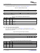
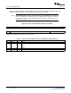
PLLC2 generates the clock from the PLL2 output clock for use by the DDR2 memory controller, as shown
in Table 5-2 .
The SYSCLK1 output clock divider value defaults to /1, resulting in a 594-MHZ DDR Phy clock (297-MHZ
DDR). It can be modified by software (using the RATIO bit in PLLDIV1) in combination with other PLL
multipliers to achieve the desired DDR2 memory controller clock rate.
Table 5-2. PLLC2 Output Clock
Output Clock Default Divider Divider Type Used by
SYSCLK1 /1 Programmable DSP Subsystem
The PLLC2 is programmed similarly to the PLLC1. Refer to the appropriate subsection on how to program
the PLL2 clocks:
• If the PLL is powered down (PLLPWRDN bit in PLLCTL is set to 1), follow the full PLL initialization
procedure in Section 5.3.2.2 to initialize the PLL.
• If the PLL is not powered down (PLLPWRDN bit in PLLCTL is cleared to 0), follow the sequence in
Section 5.3.2.3 to change the PLL multiplier.
• If the PLL is already running at a desired multiplier and only the SYSCLK divider needs to be changed,
follow the sequence in Section 5.3.2.4 .
Note that the PLL is powered down after the following device-level global resets:
• Power-on Reset ( POR)
• Warm Reset ( RESET)
• Max Reset
In addition, note that the PLL2 frequency directly affects the DDR2 memory controller. The DDR2 memory
controller requires a special sequence to be followed before and after changing the PLL2 frequency.
Follow the additional considerations for the DDR2 memory controller in Section 5.3.2.1 , in order to not
corrupt DDR2 memory controller operation.
Before changing PLL2 and/or PLLC2 frequency, take the DDR2 memory controller requirements into
account. If the DDR2 memory controller is used in the system, follow the additional steps in this section to
change PLL2 and/or PLLC2 frequency without corrupting DDR2 memory controller operation.
• If the DDR2 memory controller is in reset when you desire to change the PLL2 frequency, follow the
steps in Section 5.3.2.1.1 .
• If the DDR2 memory controller is already out of reset when you desire to change the PLL2 frequency,
follow the steps in Section 5.3.2.1.2 .
This section discusses the steps to change the PLL2 frequency when the DDR2 memory controller is in
reset. Note that the DDR2 memory controller is in reset after these device-level global resets: power-on
reset ( POR), warm reset ( RESET), and max reset.
1. Leave the DDR2 memory controller in reset.
2. Program the PLL2 clocks by following the steps in the appropriate section: Section 5.3.2.2 ,
Section 5.3.2.3 , or Section 5.3.2.4 . (Discussion in Section 5.3.2 explains which is the appropriate
subsection).
3. Initialize the DDR2 memory controller. The steps for DDR2 memory controller initialization are found in
the TMS320DM646x DMSoC DDR2 Memory Controller User's Guide (SPRUEQ4 ).
PLL Controller42 SPRUEP9A – May 2008
Submit Documentation Feedback