
User manual

5.3 PLL2 Control
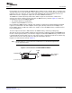
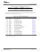
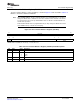
PLLDIV1(/1Prog)
PLL2_SYSCLK1
(DDR2_PHY)
1
0
PLLEN
PLL
PLLM
CLKIN/OSCIN
(A)
(A) AsselectedbythePLL2PLLCTL register
PLLOUT
www.ti.com
PLL2 Control
PLL2 provides the clock from which the DDR2 memory controller clock is derived. This is a separate clock
system from the PLL1 clocks provided to other components of the system. This dedicated clock allows the
reduction of the core clock rates to save power while maintaining the required minimum clock rate for
DDR2. PLL2 must be configured to output a 2x clock to the DDR2 PHY interface.
The DDR2 PLL controller (PLLC2) controls PLL2, which accepts the clock from the oscillator and
generates the various frequency clocks needed for the DDR2 memory controller. Figure 5-3 shows the
customization of PLL2 in the DM646x DMSoC.
• The SYSCLK divider is programmable.
• AUXCLK and SYSCLKBP are not used.
PLL2 supplies the DDR2 memory controller clock. Software controls PLL2 operation through the PLLC2
registers. The PLLM bits in the PLL multiplier control register (PLLM) control the PLL2 multiplier. The
PLL2 multiplier may be modified by software (for example, to tune the DDR2 memory controller interface
for best performance).
The PLL2 output clock must be divided-down to the DDR2 memory controller operating range.
At power-up, PLL2 is powered-down and must be powered-up by software through the PLLPWRDN bit in
the PLL control register (PLLCTL). The PLLC2 is in bypass mode and the DDR2 memory controller clock
is provided directly from the input reference clock. Once the PLL is powered-up and locked, software may
switch the device to PLL mode operation by setting the PLLEN bit in PLLCTL.
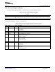
Registers used in PLLC2 are listed in Table 5-4 .
Note: PLLDIV1 defaults to /1 at reset and can be modified after reset. PLLDIV2 through PLLDIV9
are not supported on PLL2.
Figure 5-3. PLL2 Structure in TMS320DM646x DMSoC
SPRUEP9A – May 2008 PLL Controller 41
Submit Documentation Feedback