
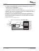
User manual


5.2.2.1 Initialization to PLL Mode from PLL Power Down
5.2.2.2 Changing PLL Multiplier
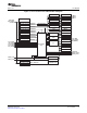
PLL1 Control
www.ti.com
If the PLL is powered down (PLLPWRDN bit in PLLCTL is set to 1), follow this procedure to change the
PLL1 frequencies. The recommendation is to stop all peripheral operation before changing the PLL1
frequency, with the exception of the ARM and DDR2 memory controller. The ARM must be operational to
program the PLL controller. The DDR2 memory controller operates off of the clock from PLLC2.
1. Select the clock mode by programming the CLKMODE bit in PLLCTL.
2. Before changing the PLL frequency, switch to PLL bypass mode:
a. Clear the PLLENSRC bit in PLLCTL to 0 to allow PLLCTL.PLLEN to take effect.
b. Clear the PLLEN bit in PLLCTL to 0 (select PLL bypass mode).
c. Wait for 20 MXI clock cycles to ensure PLLC switches to bypass mode properly.
3. Set the PLLRST bit in PLLCTL to 1 (reset PLL).
4. Set the PLLDIS bit in PLLCTL to 1 (disable PLL output).
5. Clear the PLLPWRDN bit in PLLCTL to 0 to bring the PLL out of power-down mode.
6. Clear the PLLDIS bit in PLLCTL to 0 (enable the PLL) to allow PLL outputs to start toggling. Note that
the PLLC is still at PLL bypass mode; therefore, the toggling PLL output does not get propagated to
the rest of the device.
7. Wait for PLL stabilization time. (4096 MXI clock cycles)
8. Program the required multiplier value in the PLL multiplier control register (PLLM).
9. Wait for PLL to reset properly. The PLL reset time is a minimum of 32 MXI clock cycles.
10. Clear the PLLRST bit in PLLCTL to 0 to bring the PLL out of reset.
11. Wait for 2000 MXI clock or reference clock cycles to allow PLL to lock.
12. Set the PLLEN bit in PLLCTL to 1 to remove the PLL from bypass mode.
If the PLL is not powered down (PLLPWRDN bit in PLLCTL is cleared to 0) and the PLL stabilization time
is previously met (step 7 in Section 5.2.2.1 ), follow this procedure to change PLL1 multiplier. The
recommendation is to stop all peripheral operation before changing the PLL multiplier, with the exception
of the ARM and DDR2 memory controller. The ARM must be operational to program the PLL controller.
The DDR2 memory controller operates off of the clock from PLLC2.
1. Before changing the PLL frequency, switch to PLL bypass mode:
a. Clear the PLLENSRC bit in PLLCTL to 0 to allow PLLCTL.PLLEN to take effect.
b. Clear the PLLEN bit in PLLCTL to 0 (select PLL bypass mode).
c. Wait for 20 MXI clock cycles to ensure PLLC switches to bypass mode properly.
2. Set the PLLRST bit in PLLCTL to 1 (reset PLL).
3. Clear the PLLDIS bit in PLLCTL to 0 (enable the PLL) to allow PLL outputs to start toggling. Note that
the PLLC is still at PLL bypass mode; therefore, the toggling PLL output does not get propagated to
the rest of the device.
4. Program the required multiplier value in the PLL multiplier control register (PLLM).
5. Wait for PLL to reset properly. The PLL reset time is a minimum of 32 MXI clock cycles.
6. Clear the PLLRST bit in PLLCTL to 0 to bring the PLL out of reset.
7. Wait for 2000 MXI clock or reference clock cycles to allow PLL to lock.
8. Set the PLLEN bit in PLLCTL to 1 to remove the PLL from bypass mode.
40 PLL Controller SPRUEP9A – May 2008
Submit Documentation Feedback