
User manual


5.2.1 Device Clock Generation
5.2.2 Steps for Changing PLL1/Core Domain Frequency
www.ti.com
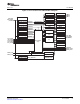
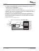
PLL1 Control
PLLC1 generates several clocks from the PLL1 output clock for use by the various processors and
modules. These are summarized in Table 5-1 .
Note: On the DM646x DMSoC, all PLL1 SYSCLK n dividers are programmable but you should not
change the divider value to maintain the clock ratios between various modules of the device.
You should only use the power-up default divider values for all PLL1 SYSCLK n dividers for
normal device operation.
PLL2 SYSCLK1 divider value is programmable and you may change the divider value for the
desired DDR2 memory controller clock frequency.
Table 5-1. PLLC1 Output Clocks
Output Clock Default Divider Divider Type Used by
SYSCLK1 /1 Programmable DSP Subsystem
SYSCLK2 /2 Programmable ARM Subsystem, EDMA, HDVICPs, DDR2 Memory
Controller, PCI, VPIFs, TSIFs, VDCE
SYSCLK3 /4 Programmable HPI, EMIFA, USB, VLYNQ, UARTs, McASPs, I2C, SPIs,
PWMs, Timers, GPIO, EMAC, CRGEN, System Module
SYSCLK4 /6 Programmable ATA
SYSCLK5 /8 Programmable TSIF1
SYSCLK6 /8 Programmable TSIF2
SYSCLK8 /8 Programmable VPIF2
SYSCLK9 /6 Programmable VLYNQ
SYSCLKBP DEV_CLKIN/n Programmable TSIFs
AUXCLK DEV_CLKIN Fixed at 27 MHZ TSIFs, VPIFs
Refer to the appropriate subsection on how to program the PLL1/Core Domain clocks:
• If the PLL is powered down (PLLPWRDN bit in PLLCTL is set to 1), follow the full PLL initialization
procedure in Section 5.2.2.1 to initialize the PLL.
• If the PLL is not powered down (PLLPWRDN bit in PLLCTL is cleared to 0), follow the sequence in
Section 5.2.2.2 to change the PLL multiplier.
• If the PLL is already running at a desired multiplier and only the SYSCLK dividers need to be changed,
follow the sequence in Section 5.3.2.4 .
Note that the PLL is powered down after the following device-level global resets:
• Power-on Reset ( POR)
• Warm Reset ( RESET)
• Max Reset
SPRUEP9A – May 2008 PLL Controller 39
Submit Documentation Feedback