
User manual


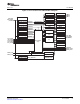

5.2 PLL1 Control
PLLDIV1(/1Prog)
PLLDIV2(/2Prog)
PLLDIV3(/4Prog)
PLLDIV4(/6Prog)
PLLDIV5(/8Prog)
PLLDIV6(/8Prog)
PLLDIV8(/8Prog)
PLLDIV9(/6Prog)
BPDIV(/1Prog)
SYSCLK1
SYSCLK2
SYSCLK3
SYSCLK4
SYSCLK5
SYSCLK6
SYSCLK8
SYSCLK9
SYSCLKBP
AUXCLK
1
0
PLLEN
PLL
1
0
CLKMODE
PLLM
CLKIN
OSCIN
PLLOUT
PLL1 Control
www.ti.com
PLL1 supplies the primary DM646x DMSoC system clock. Software controls the PLL1 operation through
the system PLL controller 1 (PLLC1) registers (base address: 1C4 0800h). Figure 5-2 shows the
customization of PLL1 in the DM646x DMSoC.
• The SYSCLK dividers are programmable (see Table 5-1 ).
• AUXCLK is the clock provided to the fixed clock domains
The PLL1 multiplier is controlled by the PLLM bit in the PLL multiplier control register (PLLM) and is set to
a default value of 15h at power-up, resulting in a PLL multiplier of 22 × . This default setting yields a
594-MHZ PLL output clock when using a 27-MHZ clock source. The PLL1 multiplier may be modified by
software (for example, set to 18 × for a 486-MHZ operation).
At power-up, PLL1 is powered-down/disabled and must be powered-up by software through the
PLLPWRDN bit in the PLL control register (PLLCTL). The system operates in bypass mode and the
system clock is provided directly from the input reference clock (CLKIN or OSCIN). Once the PLL is
powered-up and locked, software can switch the device to PLL mode operation. Set the PLLEN bit in
PLLCTL to enable the PLL.
Registers used in PLLC1 are listed in Table 5-4
Figure 5-2. PLL1 Structure in the TMS320DM646x DMSoC
PLL Controller38 SPRUEP9A – May 2008
Submit Documentation Feedback