
User manual


10.4.2 PLL and Clock Configuration
Default Device Configurations
www.ti.com
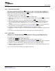
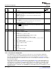
Table 10-3. Boot Configuration Register (BOOTCFG) Field Descriptions
Latched pin at
the rising edge
of RESET or
Bit Field Value Description POR
31-18 Reserved 0 Reserved. Read returns 0.
17 DSP_BT DSP Boot. This bit causes the DSP to be released from reset automatically. The DSPBOOT
C64x+ boots from EMIFA (default DSPBOOTADDR address 0x4220 0000). If
BOOTMODE = 2h or 3h,
or PCIEN = 1, then the C64x+ self-boot will fail since EMIFA will be disabled.
0 ARM boots C64x+ DSP.
1 C64x+ DSP self-boots.
16 PCIEN PCI Enable. PCIEN
0 PCI is disabled.
1 PCI is enabled. The internal pullup and pulldown resistors on the PCI pins are
disabled and configures the pin multiplexing for PCI.
15-9 Reserved 0 Reserved. Read returns 0.
8 CS2_BW EMIFA EM_CS2 Default Bus Width. This bit determines the default bus width of the CS2BW
EMIFA EM_CS2 memory space. This ensures that boot from EMIFA (ARM or DSP)
correctly reads the attached memory.
0 Default to 8-bit operation.
1 Default to 16-bit operation.
7-4 Reserved 0 Reserved. Read returns 0.
3-0 BOOTMODE 0-Fh Boot Mode Configuration. BTMODE[3:0]
0 Emulation boot. (BOOT from ROM)
1h Reserved
2h HPI-16 (if PCIEN = 0). (BOOT from ROM)
PCI without autoinitialization (if PCIEN = 1). (BOOT from ROM)
3h HPI-32 (if PCIEN = 0). (BOOT from ROM)
PCI with autoinitialization (if PCIEN = 1). (BOOT from ROM)
4h EMIFA direct boot (ROM/NOR) (if PCIEN = 0; error if PCIEN = 1, defaults to UART0).
5h Reserved
6h I2C boot. (BOOT from ROM)
7h NAND Flash boot (if PCIEN = 0; error if PCIEN = 1).
8h UART0 boot. (BOOT from ROM)
9h Reserved
Ah VLYNQ boot. (BOOT from ROM)
Bh Reserved
Ch-Dh Reserved
Eh SPI boot. (BOOT from ROM)
Fh Reserved
After POR, Warm reset, and Max reset, the PLLs and clocks are set to their default configurations.
The PLLs are in bypass mode and disabled by default. This means that the input reference clock at
DEV_MXI (typically 27 MHz) drives the chip after reset. For more information, see Chapter 5 and the
device-specific data manual. The default state of the PLLs is reflected by the default state of the register
bits in the PLLC registers.
Only a subset of module clocks are enabled after reset by default. Table 6-1 shows which modules are
enabled after reset. As shown in Table 6-1 , the following modules are enabled by default: ARM, Timer2
(watchdog timer), System Module, and ARM interrupt controller. Some modules are enabled by default
depending on the sampled state of the device configuration pins. For example, EMIFA is enabled after
reset when the device configuration pins (BTMODE[3:0] = 0100, EMIFA direct boot and PCIEN = 0) select
EMIFA boot mode.
116 Reset SPRUEP9A – May 2008
Submit Documentation Feedback