
Datasheet


Table Of Contents
V
DD
GND
X
IN
Xout
SSC_SEL 0
SSC_SEL 1
FS
XO
Control
Logic
x1orx4
SSC
LV
Cmos
OUT
3 Quick Start
4 EVM Hardware
4.1 Hardware Configuration
4.1.1 Power Supply
4.1.1.1 USB Power Supply
4.1.1.2 External Power Supply
www.ti.com
Quick Start
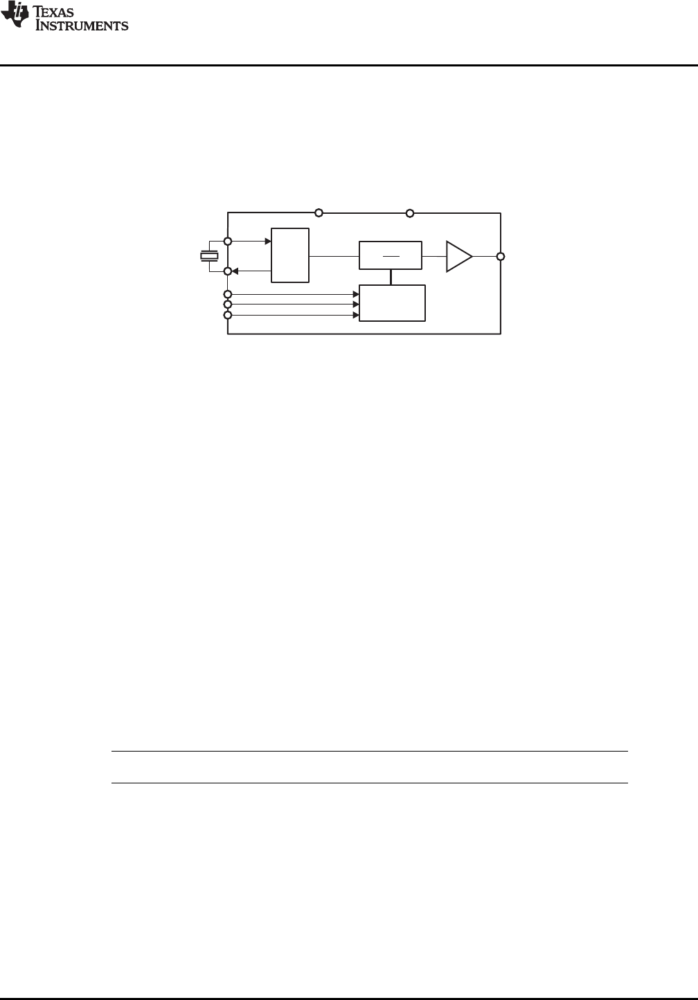
By modifying the clock signal, the device can generate output frequencies between 8MHz and 108MHz
with or without SSC from a fundamental mode crystal.
In x1 Mode with an SSC amount of 0%, the device works as a standard crystal oscillator and does not
make use of the built in PLL.
The CDCS502 operates in 3.3V environment and it is characterized for operation from –40 ° C to 85 ° C. The
device is offered in an 8 Pin TSSOP package.
Figure 3. Functional Block Diagram of the CDCS502
The following steps allow the user to get started quickly with the EVM.
1. Connect the EVM with the PC with a USB cable or supply 3.3V using connectors J20 and J21.
2. Select the amount of Spread Spectrum and the frequency multiplication using jumpers J32, J33 and
J25.
3. The desired output is available on J5
This section gives an extended description of the board hardware, providing the user with a
comprehensive overview of its configuration. Detailed information regarding onboard jumpers and
solder-bridges are included. The user may change the setup and configure the device according to their
requirements.
Power for the EVM can be supplied fully with a USB power supply or a stabilized external power supply.
The following paragraphs describe how to set the board jumpers for each power supply option.
Note: All EVMs are delivered with USB power supply as default
Jumper J19 must be on and jumper J17 must be off. With this configuration the DC/DC converter
generates the 3.3V necessary for the CDCS502 out of the 5V from the USB connector. Data lines from
the USB are not used.
For external power supply jumper J19 must be off. Only with this action an external power supply can be
used.
SCAU028 – April 2009 CDCS502 Performance Evaluation Module 3
Submit Documentation Feedback