
Datasheet


Table Of Contents
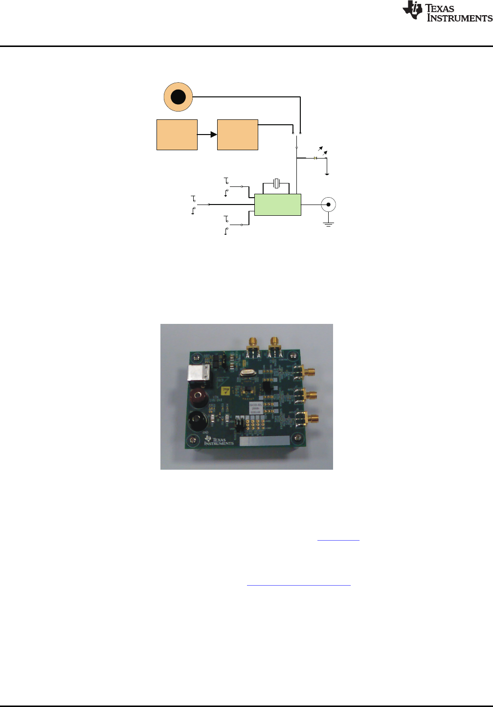
1 Block Diagram
USB
Connector
3.3VConnector
3.3V
DC/DC
CDCS502
Output
3.3V
3.3V
3.3V
SSC_0
SSC_1
FS
V
DD
Crystal
1.1 Features
1.2 Related Documentation
1.3 Additional Assistance
2 About the CDCS502
Block Diagram
www.ti.com
Figure 1. CDCS502 Simplified Block Diagram
• Easy-to-use evaluation module for fast prototyping and application evaluation of the CDCS502
• Option for USB power or external power supply
Figure 2. CDCS502 Printed-Circuit Board
CDCS502 Crystal Oscillator / Clock Generator with optional SSC (SCAS868 )
For assistance with this device, send an e-mail to clocks_apps@list.ti.com
The CDCS502 is a spread spectrum capable, fundamental mode crystal oscillator with selectable
frequency multiplication.
The crystal frequency is processed by a PLL, whose output frequency is either equal to the input
frequency or multiplied by a factor of 4.
The PLL is also able to spread the clock signal by ± 0%, ± 0.5%, ± 1% or ± 2% centered on the output clock
frequency with a triangular modulation.
2 CDCS502 Performance Evaluation Module SCAU028 – April 2009
Submit Documentation Feedback