
Datasheet


Table Of Contents
- FEATURES
- APPLICATIONS
- DESCRIPTION
- DEVICE INFORMATION
- ABSOLUTE MAXIMUM RATINGS
- THERMAL RESISTANCE FOR TSSOP (PW) PACKAGE
- RECOMMENDED OPERATING CONDITIONS
- RECOMMENDED CRYSTAL/VCXO SPECIFICATIONS
- EEPROM SPECIFICATION
- TIMING REQUIREMENTS
- DEVICE CHARACTERISTICS
- DEVICE CHARACTERISTICS (Continued)
- DEVICE CHARACTERISTICS (Continued)
- PARAMETER MEASUREMENT INFORMATION
- TYPICAL CHARACTERISTICS
- APPLICATION INFORMATION
- Control Terminal Configuration
- DEFAULT DEVICE SETTING
- SDA/SCL SERIAL INTERFACE
- DATA PROTOCOL
- Generic Programming Sequence
- Byte Write Programming Sequence
- Byte Read Programming Sequence
- Block Write Programming Sequence
- Block Read Programming Sequence
- Timing Diagram for the SDA/SCL Serial Control Interface
- SDA/SCL Hardware Interface
- SDA/SCL CONFIGURATION REGISTERS
- PLL MULTIPLIER/DIVIDER DEFINITIONPLL settings limits: 16≤q≤63, 0≤p≤7, 0≤r≤511 to PLL Multiplier/Divider Definition Section
- Revision History
CDCE949
CDCEL949
www.ti.com
SCAS844D –AUGUST 2007–REVISED MARCH 2010
APPLICATION INFORMATION
Control Terminal Configuration
The CDCE949/CDCEL949 has three user-definable control terminals (S0, S1 and S2) which allow external
control of device settings. They can be programmed to perform any of the following functions:
• Spread-Spectrum Clocking selection: Spread-type and spread-amount selection
• Frequency selection: Switching between any of two user-defined frequencies
• Output-State selection: Output configuration and power-down control
The user can predefine up to eight different control settings. Table 1 and Table 2 explain these settings.
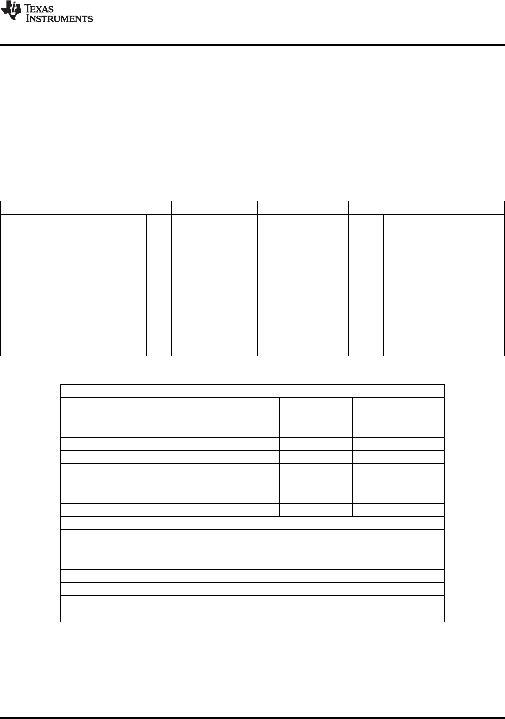
Table 1. Control Terminal Definition
External Control-Bits PLL1 Setting PLL2 Setting PLL3 Setting PLL4 Setting Y1 Setting
Control Function
SSC Selection
SSC Selection
SSC Selection
SSC Selection
Output Y2/Y3 Selection
Output Y4/Y5 Selection
Output Y6/Y7 Selection
Output Y8/Y9 Selection
PLL Frequency Selection
PLL Frequency Selection
PLL Frequency Selection
PLL Frequency Selection
Output Y1 and Power Down Selection
Table 2. PLLx Setting (can be selected for each PLL individual)
(1)
SSC Selection (Center/Down)
SSCx [3-bits] Center Down
0 0 0 0% (off) 0% (off)
0 0 1 ±0.25% –0.25%
0 1 0 ±0.5% –0.5%
0 1 1 ±0.75% –0.75%
1 0 0 ±1.0% –1.0%
1 0 1 ±1.25% –1.25%
1 1 0 ±1.5% –1.5%
1 1 1 ±2.0% –2.0%
FREQUENCY SELECTION
(2)
FSx FUNCTION
0 Frequency0
1 Frequency1
OUTPUT SELECTION
(3)
(Y2 ... Y9)
YxYx FUNCTION
0 State0
1 State1
(1) Center/Down-Spread, Frequency0/1 and State0/1 are user-definable in PLLx Configuration Register;
(2) Frequency0 and Frequency1 can be any frequency within the specified f
VCO
range.
(3) State0/1 selection is valid for both outputs of the corresponding PLL module and can be power down,
3-state, low or active
Copyright © 2007–2010, Texas Instruments Incorporated Submit Documentation Feedback 9
Product Folder Link(s): CDCE949 CDCEL949