
Datasheet


Table Of Contents
- FEATURES
- APPLICATIONS
- DESCRIPTION
- DEVICE INFORMATION
- ABSOLUTE MAXIMUM RATINGS
- THERMAL RESISTANCE FOR TSSOP (PW) PACKAGE
- RECOMMENDED OPERATING CONDITIONS
- RECOMMENDED CRYSTAL/VCXO SPECIFICATIONS
- EEPROM SPECIFICATION
- TIMING REQUIREMENTS
- DEVICE CHARACTERISTICS
- DEVICE CHARACTERISTICS (Continued)
- DEVICE CHARACTERISTICS (Continued)
- PARAMETER MEASUREMENT INFORMATION
- TYPICAL CHARACTERISTICS
- APPLICATION INFORMATION
- Control Terminal Configuration
- DEFAULT DEVICE SETTING
- SDA/SCL SERIAL INTERFACE
- DATA PROTOCOL
- Generic Programming Sequence
- Byte Write Programming Sequence
- Byte Read Programming Sequence
- Block Write Programming Sequence
- Block Read Programming Sequence
- Timing Diagram for the SDA/SCL Serial Control Interface
- SDA/SCL Hardware Interface
- SDA/SCL CONFIGURATION REGISTERS
- PLL MULTIPLIER/DIVIDER DEFINITIONPLL settings limits: 16≤q≤63, 0≤p≤7, 0≤r≤511 to PLL Multiplier/Divider Definition Section
- Revision History
CDCE949
CDCEL949
www.ti.com
SCAS844D –AUGUST 2007–REVISED MARCH 2010
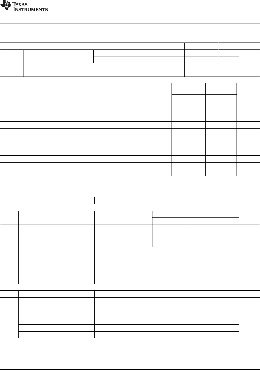
TIMING REQUIREMENTS
over recommended ranges of supply voltage, load and operating free-air temperature
CLK_IN Requirements MIN NOM MAX UNIT
PLL Bypass Mode 0 160
f
(CLK)
LVCMOS clock input frequency MHz
PLL Mode 8 160
t
r
/ t
f
Rise and fall time CLK signal (20% to 80%) 3 ns
duty
CLK
Duty cycle CLK at V
DD
/ 2 40% 60%
STANDARD FAST
MODE MODE
SDA/SCL TIMING REQUIREMENTS (see Figure 12) UNIT
MIN MAX MIN MAX
f
(SCL)
SCL clock frequency 0 100 0 400 kHz
t
su(START)
START setup time (SCL high before SDA low) 4.7 0.6 ms
t
h(START)
START hold time (SCL low after SDA low) 4 0.6 ms
t
w(SCLL)
SCL low-pulse duration 4.7 1.3 ms
t
w(SCLH)
SCL high-pulse duration 4 0.6 ms
t
h(SDA)
SDA hold time (SDA valid after SCL low) 0 3.45 0 0.9 ms
t
su(SDA)
SDA setup time 250 100 ns
t
r
SCL/SDA input rise time 1000 300 ns
t
f
SCL/SDA input fall time 300 300 ns
t
su(STOP)
STOP setup time 4.0 0.6 ms
t
BUF
Bus free time between a STOP and START condition 4.7 1.3 ms
DEVICE CHARACTERISTICS
over recommended operating free-air temperature range (unless otherwise noted)
PARAMETER TEST CONDITIONS MIN TYP
(1)
MAX UNIT
OVERALL PARAMETER
All PLLs on 38
All outputs off, f
CLK
= 27
I
DD
Supply current (see Figure 3) mA
MHz, f
VCO
= 135 MHz;
Per PLL 9
CDCE949
4
V
DDOUT
=3.3 V
Supply current (see Figure 4 and No load, all outputs on,
I
DD(OUT)
mA
Figure 5) f
out
= 27 MHz
CDCEL949
2
V
DDOUT
=1.8 V
Power down current. Every circuit
I
DD(PD)
f
IN
= 0 MHz, V
DD
= 1.9 V 50 mA
powered down except SDA/SCL
Supply voltage V
DD
threshold for power
V
(PUC)
0.85 1.45 V
up control circuit
f
VCO
VCO frequency range of PLL 80 230 MHz
f
OUT
LVCMOS output frequency 230 MHz
LVCMOS PARAMETER
V
IK
LVCMOS input voltage V
DD
= 1.7 V; I
I
= –18 mA –1.2 V
I
I
LVCMOS input current V
I
= 0 V or V
DD
; V
DD
= 1.9 V ±5 mA
I
IH
LVCMOS input current for S0/S1/S2 V
I
= V
DD
; V
DD
= 1.9 V 5 mA
I
IL
LVCMOS input current for S0/S1/S2 V
I
= 0 V; V
DD
= 1.9 V –4 mA
Input capacitance at Xin/Clk V
ICLK
= 0 V or V
DD
6
C
I
Input capacitance at Xout V
IXout
= 0 V or V
DD
2 pF
Input capacitance at S0/S1/S2 V
IS
= 0 V or V
DD
3
(1) All typical values are at respective nominal V
DD
.
Copyright © 2007–2010, Texas Instruments Incorporated Submit Documentation Feedback 5
Product Folder Link(s): CDCE949 CDCEL949