
Datasheet


Table Of Contents
- FEATURES
- APPLICATIONS
- DESCRIPTION
- DEVICE INFORMATION
- ABSOLUTE MAXIMUM RATINGS
- THERMAL RESISTANCE FOR TSSOP (PW) PACKAGE
- RECOMMENDED OPERATING CONDITIONS
- RECOMMENDED CRYSTAL/VCXO SPECIFICATIONS
- EEPROM SPECIFICATION
- TIMING REQUIREMENTS
- DEVICE CHARACTERISTICS
- DEVICE CHARACTERISTICS (Continued)
- DEVICE CHARACTERISTICS (Continued)
- PARAMETER MEASUREMENT INFORMATION
- TYPICAL CHARACTERISTICS
- APPLICATION INFORMATION
- Control Terminal Configuration
- DEFAULT DEVICE SETTING
- SDA/SCL SERIAL INTERFACE
- DATA PROTOCOL
- Generic Programming Sequence
- Byte Write Programming Sequence
- Byte Read Programming Sequence
- Block Write Programming Sequence
- Block Read Programming Sequence
- Timing Diagram for the SDA/SCL Serial Control Interface
- SDA/SCL Hardware Interface
- SDA/SCL CONFIGURATION REGISTERS
- PLL MULTIPLIER/DIVIDER DEFINITIONPLL settings limits: 16≤q≤63, 0≤p≤7, 0≤r≤511 to PLL Multiplier/Divider Definition Section
- Revision History
EEPROM
Xin/CLK
Xout
V
DD
GND
Vctr
V
DDOUT
VCXO
XO
LVCMOS
Y2
Y1
Y3
LV
CMOS
Pdiv1
10-Bit
Y4
Y5
Y6
Y7
Y8
Y9
LV
CMOS
Pdiv9
7-Bit
Pdiv8
7-Bit
M8
M9
LV
CMOS
LV
CMOS
Pdiv7
7-Bit
Pdiv6
7-Bit
M6
M7
LV
CMOS
LV
CMOS
Pdiv5
7-Bit
Pdiv4
7-Bit
M4
M5
LV
CMOS
LV
CMOS
Pdiv3
7-Bit
Pdiv2
7-Bit
M2
M3
LV
CMOS
Programming
and
SDA/SCL
Register
InputClock
M1
PLL Bypass
PLL 1
withSSC
MU
X1
PLL Bypass
PLL 2
withSSC
MUX2
PLL Bypass
PLL 3
withSSC
M
UX3
PLL Bypass
PLL 4
withSSC
M
UX4
S0
S1/SDA
S2/SCL
CDCE949
CDCEL949
www.ti.com
SCAS844D –AUGUST 2007–REVISED MARCH 2010
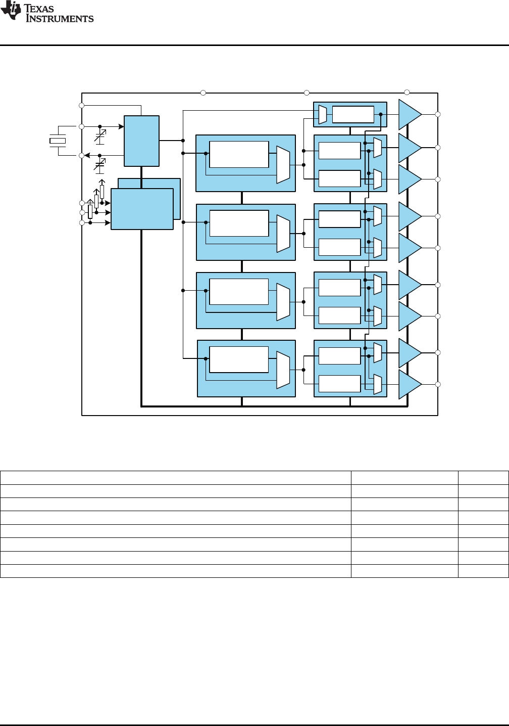
FUNCTIONAL BLOCK DIAGRAM
ABSOLUTE MAXIMUM RATINGS
over operating free-air temperature range (unless otherwise noted)
(1)
VALUE UNIT
V
DD
Supply voltage range –0.5 to 2.5 V
V
I
Input voltage range
(2) (3)
–0.5 to V
DD
+ 0.5 V
V
O
Output voltage range
(2)
–0.5 to V
DDOUT
+ 0.5 V
I
I
Input current (V
I
< 0, V
I
> V
DD
) 20 mA
I
O
Continuous output current 50 mA
T
stg
Storage temperature range –65 to 150 °C
T
J
Maximum junction temperature 125 °C
(1) Stresses beyond those listed under absolute maximum ratings may cause permanent damage to the device. These are stress ratings
only and functional operation of the device at these or any other conditions beyond those indicated under recommended operating
conditions is not implied. Exposure to absolute–maximum–rated conditions for extended periods may affect device reliability.
(2) The input and output negative voltage ratings may be exceeded if the input and output clamp–current ratings are observed.
(3) SDA and SCL can go up to 3.6V as stated in the Recommended Operating Conditions table.
Copyright © 2007–2010, Texas Instruments Incorporated Submit Documentation Feedback 3
Product Folder Link(s): CDCE949 CDCEL949