
Datasheet


Table Of Contents
- FEATURES
- APPLICATIONS
- DESCRIPTION
- DEVICE INFORMATION
- ABSOLUTE MAXIMUM RATINGS
- THERMAL RESISTANCE FOR TSSOP (PW) PACKAGE
- RECOMMENDED OPERATING CONDITIONS
- RECOMMENDED CRYSTAL/VCXO SPECIFICATIONS
- EEPROM SPECIFICATION
- TIMING REQUIREMENTS
- DEVICE CHARACTERISTICS
- DEVICE CHARACTERISTICS (Continued)
- DEVICE CHARACTERISTICS (Continued)
- PARAMETER MEASUREMENT INFORMATION
- TYPICAL CHARACTERISTICS
- APPLICATION INFORMATION
- Control Terminal Configuration
- DEFAULT DEVICE SETTING
- SDA/SCL SERIAL INTERFACE
- DATA PROTOCOL
- Generic Programming Sequence
- Byte Write Programming Sequence
- Byte Read Programming Sequence
- Block Write Programming Sequence
- Block Read Programming Sequence
- Timing Diagram for the SDA/SCL Serial Control Interface
- SDA/SCL Hardware Interface
- SDA/SCL CONFIGURATION REGISTERS
- PLL MULTIPLIER/DIVIDER DEFINITIONPLL settings limits: 16≤q≤63, 0≤p≤7, 0≤r≤511 to PLL Multiplier/Divider Definition Section
- Revision History
CDCE949
CDCEL949
www.ti.com
SCAS844D –AUGUST 2007–REVISED MARCH 2010
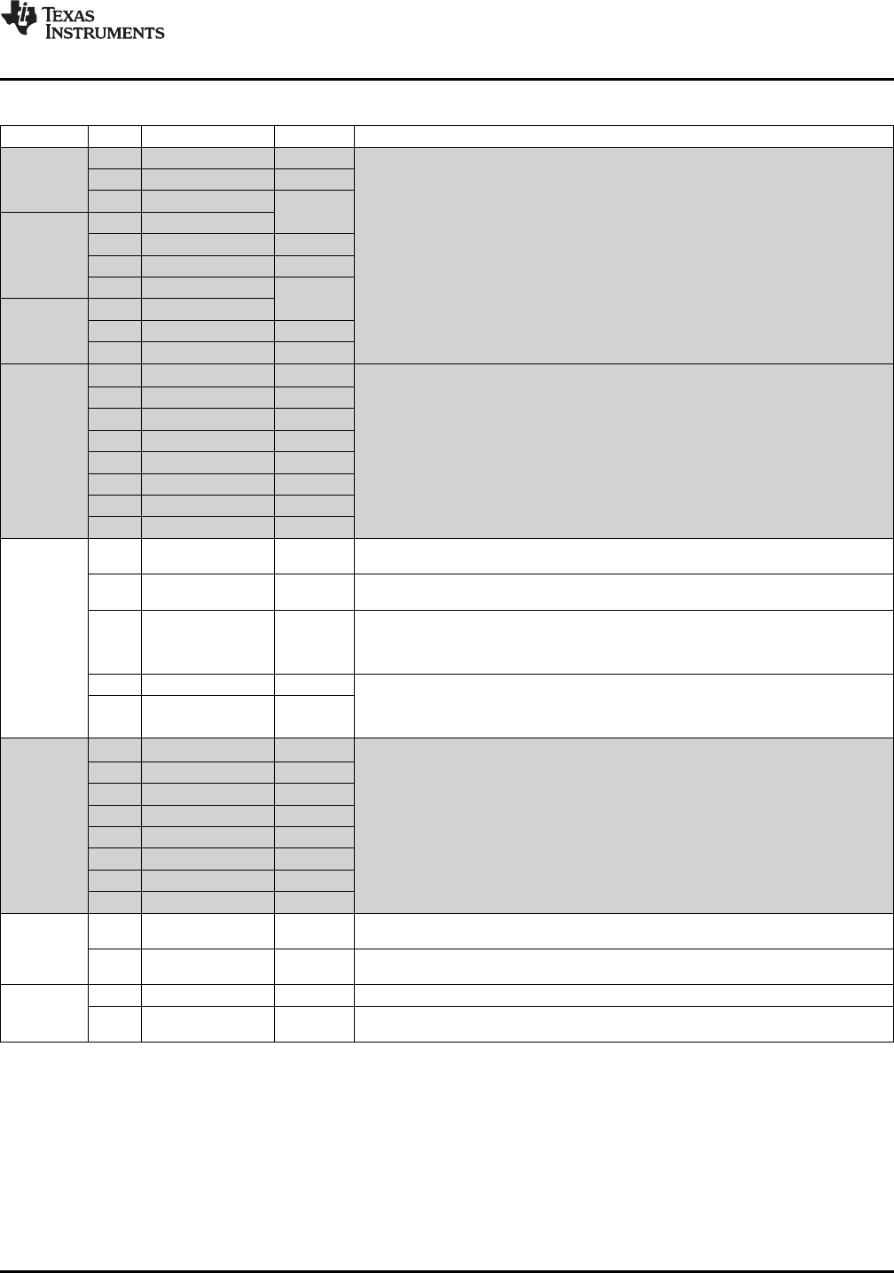
Table 11. PLL2 Configuration Register
OFFSET
(1)
Bit
(2)
Acronym Default
(3)
DESCRIPTION
20h 7:5 SSC2_7 [2:0] 000b SSC2: PLL2 SSC Selection (Modulation Amount)
(4)
4:2 SSC2_6 [2:0] 000b Down Center
000 (off) 000 (off)
1:0 SSC2_5 [2:1]
001 – 0.25% 001 ± 0.25%
000b
010 – 0.5% 010 ± 0.5%
21h 7 SSC2_5 [0]
011 – 0.75% 011 ± 0.75%
6:4 SSC2_4 [2:0] 000b
100 – 1.0% 100 ± 1.0%
101 – 1.25% 101 ± 1.25%
3:1 SSC2_3 [2:0] 000b
110 – 1.5% 110 ± 1.5%
0 SSC2_2 [2]
111 – 2.0% 111 ± 2.0%
000b
22h 7:6 SSC2_2 [1:0]
5:3 SSC2_1 [2:0] 000b
2:0 SSC2_0 [2:0] 000b
23h
7 FS2_7 0b
FS2_x: PLL2 Frequency Selection
(4)
6 FS2_6 0b 0 – f
VCO2_0
(predefined by PLL2_0 – Multiplier/Divider value)
1 – f
VCO2_1
(predefined by PLL2_1 – Multiplier/Divider value)
5 FS2_5 0b
4 FS2_4 0b
3 FS2_3 0b
2 FS2_2 0b
1 FS2_1 0b
0 FS2_0 0b
24h PLL2 Multiplexer: 0 – PLL2
7 MUX2 1b
1 – PLL2 Bypass (PLL2 is in power down)
Output Y4 Multiplexer: 0 – Pdiv2
6 M4 1b
1 – Pdiv4
Output Y5 Multiplexer: 00 – Pdiv2-Divider
01 – Pdiv4-Divider
5:4 M5 10b
10 – Pdiv5-Divider
11 – reserved
3:2 Y4Y5_ST1 11b Y4, 00 – Y4/Y5 disabled to 3-State (PLL2 is in power down)
Y5-State0/1definition: 01 – Y4/Y5 disabled to 3-State (PLL2 on)
10–Y4/Y5 disabled to low (PLL2 on)
1:0 Y4Y5_ST0 01b
11 – Y4/Y5 enabled (normal operation, PLL2 on)
25h
7 Y4Y5_7 0b
Y4Y5_x Output State Selection
(4)
6 Y4Y5_6 0b 0 – state0 (predefined by Y4Y5_ST0)
1 – state1 (predefined by Y4Y5_ST1)
5 Y4Y5_5 0b
4 Y4Y5_4 0b
3 Y4Y5_3 0b
2 Y4Y5_2 0b
1 Y4Y5_1 1b
0 Y4Y5_0 0b
26h PLL2 SSC down/center selection: 0 – down
7 SSC2DC 0b
1 – center
7-Bit Y4-Output-Divider Pdiv4: 0 – reset and stand-by
6:0 Pdiv4 01h
1-to-127 – divider value
27h 7 — 0b Reserved – do not write others than 0
7-Bit Y5-Output-Divider Pdiv5: 0 – reset and stand-by
6:0 Pdiv5 01h
1-to-127 – divider value
(1) Writing data beyond 50h may adversely affect device function.
(2) All data is transferred MSB-first.
(3) Unless a custom setting is used
(4) The user can pre-define up to eight different control settings. In normal device operation, these settings can be selected by the external
control pins, S0, S1, and S2.
Copyright © 2007–2010, Texas Instruments Incorporated Submit Documentation Feedback 19
Product Folder Link(s): CDCE949 CDCEL949