
Datasheet


Table Of Contents
- FEATURES
- APPLICATIONS
- DESCRIPTION
- DEVICE INFORMATION
- ABSOLUTE MAXIMUM RATINGS
- THERMAL RESISTANCE FOR TSSOP (PW) PACKAGE
- RECOMMENDED OPERATING CONDITIONS
- RECOMMENDED CRYSTAL/VCXO SPECIFICATIONS
- EEPROM SPECIFICATION
- TIMING REQUIREMENTS
- DEVICE CHARACTERISTICS
- DEVICE CHARACTERISTICS (Continued)
- DEVICE CHARACTERISTICS (Continued)
- PARAMETER MEASUREMENT INFORMATION
- TYPICAL CHARACTERISTICS
- APPLICATION INFORMATION
- Control Terminal Configuration
- DEFAULT DEVICE SETTING
- SDA/SCL SERIAL INTERFACE
- DATA PROTOCOL
- Generic Programming Sequence
- Byte Write Programming Sequence
- Byte Read Programming Sequence
- Block Write Programming Sequence
- Block Read Programming Sequence
- Timing Diagram for the SDA/SCL Serial Control Interface
- SDA/SCL Hardware Interface
- SDA/SCL CONFIGURATION REGISTERS
- PLL MULTIPLIER/DIVIDER DEFINITIONPLL settings limits: 16≤q≤63, 0≤p≤7, 0≤r≤511 to PLL Multiplier/Divider Definition Section
- Revision History
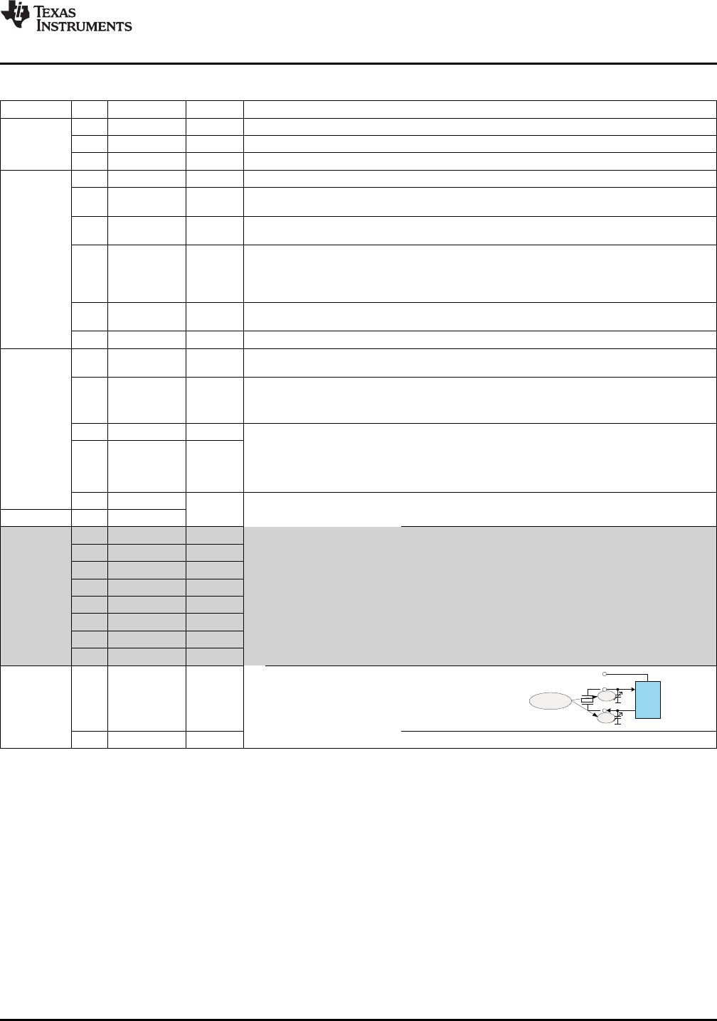
Xin
Xout
Vctr
VCXO
XO
20pF
20pF
i.e.
XCSEL =10pF
CDCE949
CDCEL949
www.ti.com
SCAS844D –AUGUST 2007–REVISED MARCH 2010
Table 9. Generic Configuration Register
OFFSET
(1)
Bit
(2)
Acronym Default
(3)
DESCRIPTION
00h 7 E_EL xb Device Identification (read only): ‘1’ is CDCE949 (3.3V), ‘0’ is CDCEL949 (1.8V)
6:4 RID Xb Revision Identification Number (read only)
3:0 VID 1h Vendor Identification Number (read only)
01h 7 – 0b Reserved - always write 0
EEPROM Programming 0 – EEPROM programming is completed
6 EEPIP 0b
Status
(4)
: (read only) 1 – EEPROM is in programming mode
Permanently Lock EEPROM 0 – EEPROM is not locked
5 EELOCK 0b
Data
(5)
: 1 – EEPROM will be permanently locked
Device power down (overwrites S0/S1/S2 setting; configuration register settings are unchanged)
Note: PWDN cannot be set to 1 in the EEPROM.
4 PWDN 0b
0 – device active (all PLLs and all outputs are enabled)
1 – device power down (all PLLs in power down and all outputs in 3-State)
Input clock selection: 00 – X-tal 10 – LVCMOS
3:2 INCLK 00b
01 – VCXO 11 – reserved
1:0 SLAVE_ADR 00b Programmable Address Bits A0 and A1 of the Slave Receiver Address
02h Clock source selection for output Y1: 0 – input clock
7 M1 1b
1 – PLL1 clock
Operation mode selection for pin 22/23
(6)
6 SPICON 0b
0 – serial programming interface SDA (pin 23) and SCL (pin 22)
1 – control pins S1 (pin 23) and S2 (pin 22)
5:4 Y1_ST1 11b Y1-State0/1 Definition (applies to Y1_ST1 and Y1_ST0)
00 – device power down (all PLLs in power down and all outputs in 3-state)
01 – Y1 disabled to 3-state
3:2 Y1_ST0 01b
10 – Y1 disabled to low
11 – Y1 enabled (normal operation)
1:0 Pdiv1 [9:8] 10-Bit Y1-Output-Divider Pdiv1: 0 – divider reset and stand-by
001h
1-to-1023 – divider value
03h 7:0 Pdiv1 [7:0]
04h 7 Y1_7 0b Y1_x State Selection
(7)
6 Y1_6 0b 0 – State0 (predefined by Y1-State0 Definition [Y1_ST0])
1 – State1 (predefined by Y1-State1 Definition [Y1_ST1])
5 Y1_5 0b
4 Y1_4 0b
3 Y1_3 0b
2 Y1_2 0b
1 Y1_1 1b
0 Y1_0 0b
05h Crystal load capacitor 00h → 0 pF
selection
(8)
: 01h → 1 pF
02h → 2 pF
7:3 XCSEL 0Ah
14h-to-1Fh → 20 pF
2:0 — 0b Reserved - do not write others than 0
(1) Writing data beyond ‘50h’ may adversely affect device function.
(2) All data is transferred MSB-first.
(3) Unless custom setting is used.
(4) During EEPROM programming, no data is allowed to be sent to the device via the SDA/SCL bus until the programming sequence is
completed. Data, however, can be read during the programming sequence (Byte Read or Block Read).
(5) If this bit is set high in the EEPROM, the actual data in the EEPROM is permanently locked, and no further programming is possible.
Data, however can still be written via SDA/SCL bus to the internal register to change device function on the fly. But new data can no
longer be saved to the EEPROM. EELOCK is effective only if written into the EEPROM
(6) Selection of control-pins is effective only if written into the EEPROM. Once written into the EEPROM, the serial programming pins are
no longer available. However, if V
DDOUT
is forced to GND, the two control-pins, S1 and S2, temporally act as serial programming pins
(SDA/SCL), and the two slave receiver address bits are reset to A0 = 0 and A1 = 0.
(7) These are the bits of the Control Terminal Register. The user can pre-define up to eight different control settings. These settings can
then be selected by the external control pins, S0, S1, and S2.
(8) The internal load capacitor (C
1
, C
2
) must be used to achieve the best clock performance. External capacitors should be used only to do
a fine adjustment of C
L
by few pF. The value of C
L
can be programmed with a resolution of 1 pF for a total crystal load range of 0 pF to
20 pF. For C
L
> 20 pF use additional external capacitors. Also, the device input capacitance must be considered; this adds 1.5 pF
(6pF//2pF) to the selected C
L
. For more information about VCXO configuration and crystal recommendations, see application report
SCAA085
Copyright © 2007–2010, Texas Instruments Incorporated Submit Documentation Feedback 15
Product Folder Link(s): CDCE949 CDCEL949