
Datasheet


Table Of Contents
- FEATURES
- APPLICATIONS
- DESCRIPTION
- DEVICE INFORMATION
- ABSOLUTE MAXIMUM RATINGS
- THERMAL RESISTANCE FOR TSSOP (PW) PACKAGE
- RECOMMENDED OPERATING CONDITIONS
- RECOMMENDED CRYSTAL/VCXO SPECIFICATIONS
- EEPROM SPECIFICATION
- TIMING REQUIREMENTS
- DEVICE CHARACTERISTICS
- DEVICE CHARACTERISTICS (Continued)
- DEVICE CHARACTERISTICS (Continued)
- PARAMETER MEASUREMENT INFORMATION
- TYPICAL CHARACTERISTICS
- APPLICATION INFORMATION
- Control Terminal Configuration
- DEFAULT DEVICE SETTING
- SDA/SCL SERIAL INTERFACE
- DATA PROTOCOL
- Generic Programming Sequence
- Byte Write Programming Sequence
- Byte Read Programming Sequence
- Block Write Programming Sequence
- Block Read Programming Sequence
- Timing Diagram for the SDA/SCL Serial Control Interface
- SDA/SCL Hardware Interface
- SDA/SCL CONFIGURATION REGISTERS
- PLL MULTIPLIER/DIVIDER DEFINITIONPLL settings limits: 16≤q≤63, 0≤p≤7, 0≤r≤511 to PLL Multiplier/Divider Definition Section
- Revision History
1 7 1 1 1 1 1 1
S Slave Address Wr A A Sr Rd A
8 1 1 1 1
ByteCountN A A A PDataByte0 … DataByteN-1
8
CommandCode
7
Slave Address
8 8
P S P
t
(BUS)
t
w(SCLL)
t
w(SCLH)
t
r
t
f
t
h(START)
t
SU(SDA)
t
h(SDA)
t
SU(STOP)
t
SU(START)
t
r
t
f
SCL
SDA
V
IH
V
IL
V
IH
V
IL
A
Bit7(MSB)
Bit6 Bit0(LSB)
R
P
Master
R
P
SDA
SCL
C
BUS
Slave
CDCE949
CDCEL949
C
BUS
CDCE949
CDCEL949
www.ti.com
SCAS844D –AUGUST 2007–REVISED MARCH 2010
Block Read Programming Sequence
Figure 11. Block Read Protocol
Timing Diagram for the SDA/SCL Serial Control Interface
Figure 12. Timing Diagram for the SDA/SCL Serial Control Interface
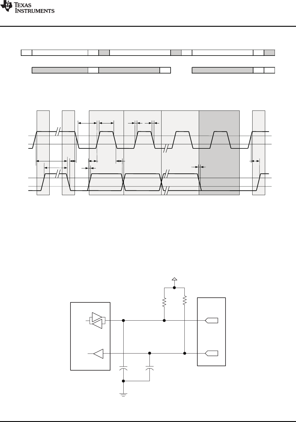
SDA/SCL Hardware Interface
Figure 13 shows how the CDCE949/CDCEL949 clock synthesizer is connected to the SDA/SCL serial interface
bus. Multiple devices can be connected to the bus but the speed may need to be reduced (400 kHz is the
maximum) if many devices are connected.
Note that the pull-up resistor value (R
P
) depends on the supply voltage, bus capacitance and number of
connected devices. The recommended pull-up value is 4.7 kΩ. It must meet the minimum sink current of 3 mA at
V
OLmax
= 0.4 V for the output stages (for more details see the SMBus or I
2
C Bus specification).
Figure 13. SDA/SCL Hardware Interface
Copyright © 2007–2010, Texas Instruments Incorporated Submit Documentation Feedback 13
Product Folder Link(s): CDCE949 CDCEL949