
Datasheet


Table Of Contents
- FEATURES
- APPLICATIONS
- DESCRIPTION
- DEVICE INFORMATION
- ABSOLUTE MAXIMUM RATINGS
- THERMAL RESISTANCE FOR TSSOP (PW) PACKAGE
- RECOMMENDED OPERATING CONDITIONS
- RECOMMENDED CRYSTAL/VCXO SPECIFICATIONS
- EEPROM SPECIFICATION
- TIMING REQUIREMENTS
- DEVICE CHARACTERISTICS
- DEVICE CHARACTERISTICS (Continued)
- DEVICE CHARACTERISTICS (Continued)
- PARAMETER MEASUREMENT INFORMATION
- TYPICAL CHARACTERISTICS
- APPLICATION INFORMATION
- Control Terminal Configuration
- DEFAULT DEVICE SETTING
- SDA/SCL SERIAL INTERFACE
- DATA PROTOCOL
- Generic Programming Sequence
- Byte Write Programming Sequence
- Byte Read Programming Sequence
- Block Write Programming Sequence
- Block Read Programming Sequence
- Timing Diagram for the SDA/SCL Serial Control Interface
- SDA/SCL Hardware Interface
- SDA/SCL CONFIGURATION REGISTERS
- PLL MULTIPLIER/DIVIDER DEFINITIONPLL settings limits: 16≤q≤63, 0≤p≤7, 0≤r≤511 to PLL Multiplier/Divider Definition Section
- Revision History
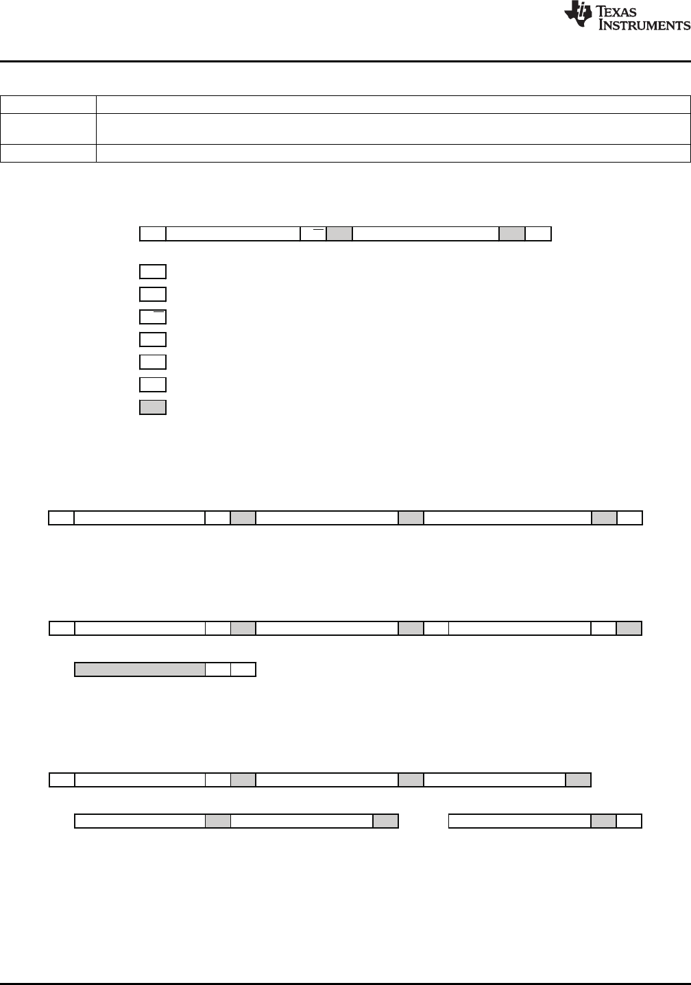
1 7 1 1 8 1 1
S Slave Address A DataByte A P
MSB LSB MSB LSB
S StartCondition
Sr RepeatedStartCondition
1=Read(Rd)fromCDCE9xxdevice;0=Write(Wr)totheCDCE9xxx
A Acknowledg(ACK=0andNACK=1)
P StopCondition
MastertoSlave Transmission
SlavetoMaster Transmission
R/W
R/W
1 7 1 1 8 1 1 1
S Slave Address Wr A A A PDataByteCommandCode
8
1 7 1 1 1 1 1 1
S Slave Address Wr A A S Rd A
8 1 1
DataByte A P
CommandCode
8 7
Slave Address
1 7 1 1 1 1
S Slave Address Wr A A A
8 1 1 1 1
DataByte0 A A A P
8
DataByteN-1…
8
DataByte1
8
CommandCode ByteCount=N
8
CDCE949
CDCEL949
SCAS844D –AUGUST 2007–REVISED MARCH 2010
www.ti.com
Table 6. Command Code Definition
BIT DESCRIPTION
0 = Block Read or Block Write operation
7
1 = Byte Read or Byte Write operation
(6:0) Byte Offset for Byte Read, Block Read, Byte Write and Block Write operation.
Generic Programming Sequence
Figure 7. Generic Programming Sequence
Byte Write Programming Sequence
Figure 8. Byte Write Protocol
Byte Read Programming Sequence
Figure 9. Byte Read Protocol
Block Write Programming Sequence
NOTE: Data Byte 0 Bits [7:0] is reserved for Revision Code and Vendor Identification. Also it is used for internal test purpose
and should not be overwritten.
Figure 10. Block Write Programming
12 Submit Documentation Feedback Copyright © 2007–2010, Texas Instruments Incorporated
Product Folder Link(s): CDCE949 CDCEL949