
Datasheet


Table Of Contents
- FEATURES
- APPLICATIONS
- DESCRIPTION
- DEVICE INFORMATION
- ABSOLUTE MAXIMUM RATINGS
- THERMAL RESISTANCE FOR TSSOP (PW) PACKAGE
- RECOMMENDED OPERATING CONDITIONS
- RECOMMENDED CRYSTAL/VCXO SPECIFICATIONS
- EEPROM SPECIFICATION
- TIMING REQUIREMENTS
- DEVICE CHARACTERISTICS
- DEVICE CHARACTERISTICS (Continued)
- DEVICE CHARACTERISTICS (Continued)
- PARAMETER MEASUREMENT INFORMATION
- TYPICAL CHARACTERISTICS
- APPLICATION INFORMATION
- Control Terminal Configuration
- DEFAULT DEVICE SETTING
- SDA/SCL SERIAL INTERFACE
- DATA PROTOCOL
- Generic Programming Sequence
- Byte Write Programming Sequence
- Byte Read Programming Sequence
- Block Write Programming Sequence
- Block Read Programming Sequence
- Timing Diagram for the SDA/SCL Serial Control Interface
- SDA/SCL Hardware Interface
- SDA/SCL CONFIGURATION REGISTERS
- PLL MULTIPLIER/DIVIDER DEFINITIONPLL settings limits: 16≤q≤63, 0≤p≤7, 0≤r≤511 to PLL Multiplier/Divider Definition Section
- Revision History
CDCE949
CDCEL949
www.ti.com
SCAS844D –AUGUST 2007–REVISED MARCH 2010
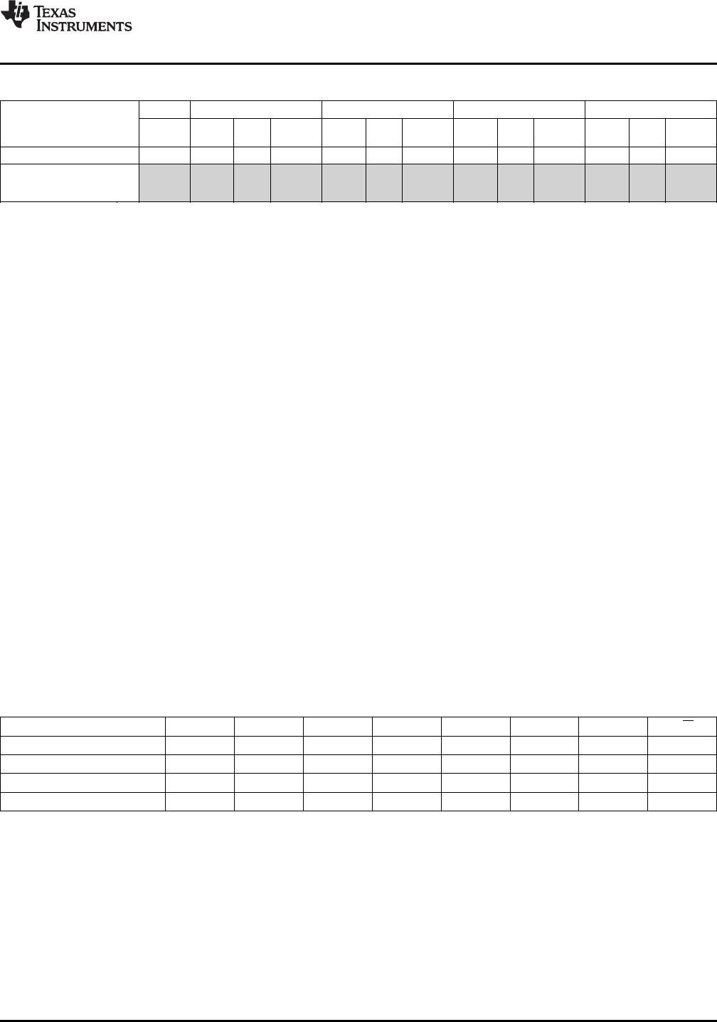
Table 4. Factory Default Setting for Control Terminal Register
Y1 PLL1 SETTING PLL2 SETTING PLL3 SETTING PLL4 SETTING
EXTERNAL
Output Freq. SSC Output Freq. SSC Output Freq. SSC Output Freq. SSC Output
CONTROL-PINS
(1)
Select Select Sel. Select Select Sel. Select Select Sel. Select Select Sel. Select
S2 S1 S0 Y1 FS1 SSC1 Y2Y3 FS2 SSC2 Y4Y5 FS3 SSC3 Y6Y7 FS4 SSC4 Y8Y9
0 3-State f
VCO1_0
off 3-State f
VCO2_0
off 3-State f
VCO3_0
off 3-State f
VCO4_0
off 3-State
SCL (I
2
C) SDA (I
2
C)
1 enabled f
VCO1_0
off enabled f
VCO2_0
off enabled f
VCO3_0
off enabled f
VCO4_0
off enabled
SCL (I
2
C) SDA (I
2
C)
(1) In default mode or when programmed respectively, S1 and S2 act as a serial programming interface, SDA/SCL. In this mode, they have
no control-pin function, but are internally interpreted as if S1=0 and S2=0. S0, however, is a control-pin which in the default mode
switches all outputs ON or OFF (as pre-defined above).
SDA/SCL SERIAL INTERFACE
The CDCE949/CDCEL949 operates as a slave device on the 2-wire serial SDA/SCL bus, compatible with the
popular SMBus or I
2
C™ specification. It operates in the standard-mode transfer (up to 100 kbps) and fast-mode
transfer (up to 400 kbps) and supports 7-bit addressing.
The S1/SDA and S2/SCL pins of the CDC9xx are dual-function pins. In the default configuration they are used as
SDA/SCL serial programming interface. They can be reprogrammed as general purpose control pins, S1 and S2,
by changing the corresponding EEPROM setting, Byte 02, Bit [6].
DATA PROTOCOL
The device supports Byte Write and Byte Read and Block Write and Block Read operations.
For Byte Write/Read operations, the system controller can individually access addressed bytes.
For Block Write/Read operations, the bytes are accessed in sequential order from lowest to highest byte (with
most significant bit first) with the ability to stop after any complete byte has been transferred. The number of
bytes read out is defined by the Byte Count field in the Generic Configuration Register. During a Block Read
instruction, the entire number of bytes defined in Byte Count must be read out to correctly finish the read cycle.
When a byte is sent to the device, it is written into the internal register and immediately takes effect. This applies
to each transferred byte, whether in a Byte Write or a Block Write sequence.
If the EEPROM Write Cycle is initiated, the internal SDA register contents are written into the EEPROM. During
this write cycle, data is not accepted at the SDA/SCL bus until the write cycle is completed. However, data can
be read during the programming sequence (Byte Read or Block Read). The programming status can be
monitored by reading EEPIP, Byte 01–Bit [6].
The offset of the indexed byte is encoded in the command code, as described in Table 6.
Table 5. Slave Receiver Address (7 bits)
Device A6 A5 A4 A3 A2 A1
(1)
A0
(1)
R/W
CDCE913/CDCEL913 1 1 0 0 1 0 1 1/0
CDCE925/CDCEL925 1 1 0 0 1 0 0 1/0
CDCE937/CDCEL937 1 1 0 1 1 0 1 1/0
CDCE949/CDCEL949 1 1 0 1 1 0 0 1/0
(1) Address bits A0 and A1 are programmable via the SDA/SCL bus (Byte 01, Bit [1:0]). This allows addressing up to 4 devices connected
to the same SDA/SCL bus. The least significant bit of the address byte designates a write or read operation.
Copyright © 2007–2010, Texas Instruments Incorporated Submit Documentation Feedback 11
Product Folder Link(s): CDCE949 CDCEL949