
Datasheet


Table Of Contents
- FEATURES
- APPLICATIONS
- DESCRIPTION
- DEVICE INFORMATION
- ABSOLUTE MAXIMUM RATINGS
- THERMAL RESISTANCE FOR TSSOP (PW) PACKAGE
- RECOMMENDED OPERATING CONDITIONS
- RECOMMENDED CRYSTAL/VCXO SPECIFICATIONS
- EEPROM SPECIFICATION
- TIMING REQUIREMENTS
- DEVICE CHARACTERISTICS
- DEVICE CHARACTERISTICS (Continued)
- DEVICE CHARACTERISTICS (Continued)
- PARAMETER MEASUREMENT INFORMATION
- TYPICAL CHARACTERISTICS
- APPLICATION INFORMATION
- Control Terminal Configuration
- DEFAULT DEVICE SETTING
- SDA/SCL SERIAL INTERFACE
- DATA PROTOCOL
- Generic Programming Sequence
- Byte Write Programming Sequence
- Byte Read Programming Sequence
- Block Write Programming Sequence
- Block Read Programming Sequence
- Timing Diagram for the SDA/SCL Serial Control Interface
- SDA/SCL Hardware Interface
- SDA/SCL CONFIGURATION REGISTERS
- PLL MULTIPLIER/DIVIDER DEFINITIONPLL settings limits: 16≤q≤63, 0≤p≤7, 0≤r≤511 to PLL Multiplier/Divider Definition Section
- Revision History
EEPROM
Xin
Xout
V
DD
GND
V
DDOUT
X-tal
Y2=27MHz
Y1=27MHz
Y3=27MHz
LV
CMOS
Pdiv1=1
Y4=27MHz
Y5=27MHz
Y6=27MHz
Y7=27MHz
Y8=27MHz
Y9=27MHz
LV
CMOS
Pdiv9=1
Pdiv8=1
M8
M9
LV
CMOS
LV
CMOS
Pdiv7=1
Pdiv6=1
M6
M7
LV
CMOS
LV
CMOS
Pdiv5=1
Pdiv4=1
M4
M5
LV
CMOS
LV
CMOS
Pdiv3=1
Pdiv2=1
M2
M3
LV
CMOS
Programming
and
SDA/SCL
Register
InputClock
M1
PLL Bypass
PLL 1
powerdown
MUX1
PLL Bypass
PLL 2
powerdown
MUX2
PLL Bypass
PLL 3
powerdown
MUX3
PLL Bypass
PLL 4
powerdown
MUX4
S0
SDA
SCL
27MHz
Crystal
ProgrammingBus
“1” =outputsenabled
“0” =outputs3-State
CDCE949
CDCEL949
SCAS844D –AUGUST 2007–REVISED MARCH 2010
www.ti.com
Table 3. Y1 Setting
(1)
Y1 SELECTION
Y1 FUNCTION
0 State 0
1 State 1
(1) State0 and State1 are user-definable in Generic Configuration
Register and can be power down, 3-state, low or active.
The S1/SDA and S2/SCL pins of the CDCE949/CDCEL949 are dual-function pins. In the default configuration
they are defined as SDA/SCL for the serial interface. They can be programmed as control pins (S1/S2) by setting
the appropriate bits in the EEPROM. Note that changes to the Control register (Bit [6] of Byte 02) have no effect
until they are written into the EEPROM.
Once they are set as control pins, the serial programming interface is no longer available. However, if V
DDOUT
is
forced to GND, the two control-pins, S1 and S2, temporarily act as serial programming pins (SDA/SCL).
S0 is not a multi-use pin, it is a control pin only.
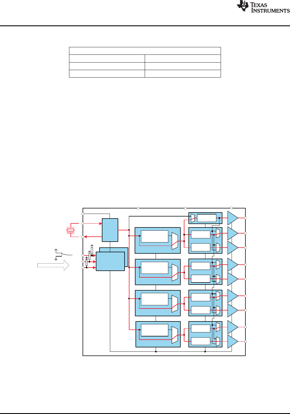
DEFAULT DEVICE SETTING
The internal EEPROM of CDCE949/CDCEL949 is preconfigured as shown in Figure 6. (The input frequency is
passed through to the output as a default.) This allows the device to operate in default mode without the extra
production step of programming it. The default setting appears after power is supplied or after a power-down/up
sequence until it is reprogrammed by the user to a different application configuration. A new register setting is
programmed via the serial SDA/SCL Interface.
Figure 6. Default Configuration
Table 4 shows the default setting for the Control Terminal Register (external control pins). In normal operation, all
8 register settings are available, but in the default configuration only the first two settings (0 and 1) can be
selected with S0, as S1 and S2 are configured as programming pins in default mode.
10 Submit Documentation Feedback Copyright © 2007–2010, Texas Instruments Incorporated
Product Folder Link(s): CDCE949 CDCEL949